CAN Bus Development: A Mock ECU
Introduction
The purpose of the Mock ECU (hereby referred to as the ME project) is to assist with remote software and hardware work on the Queen’s Formula Team. Most embedded software for the racecar interacts with the Engine Control Unit (ECU) and the Power Distribution Module (PDM). Both devices employ CAN bus as their primary communication interface with other electronics on the car, which include the dashboard, sensors and steering wheel. The ECU broadcasts engine information onto the CAN bus such as RPM, temperatures etc. The PDM provides information on the car’s power consumption with metrics such as battery voltage and current draw on the PDM’s various outputs. The objective in constructing a Mock ECU is to build a device with fully featured CAN bus outputs and power monitoring capabilities, thus emulating the same environment a team member’s project would be connected to on the car. The ME has an on board MCU which can be programmed to emit CAN messages with the same format and identifiers as the ECU and PDM. Power consumption can be measured from the 12 V output of the ME, which matches the 12 V outputs available from the real PDM. Characterizing power consumption is important on custom electronics as the car’s battery can be drained on the car very quickly. Moreover, the team has transitioned to a small single cylinder motorcycle engine whose alternator does not support the same power consumption. Reducing and fully characterizing the power consumption of the car is part of a broader goal of the electrical team to improve data acquisition. Currently, the car runs a single CAN bus but the ME accommodates two CAN buses, which will likely be required as more sensors and more data needs be moved between devices during operation.
Design
The schematic design of the ME is broken down into several sub-circuits in a multi-sheet design on Altium. The following sections break down each component of the ME schematic design.
Buck Regulator
In order to obtain a 5 V power supply from the 12 V input, a buck regulator is
employed. In past designs, I have employed so called “LDO” regulators. LDO
regulators are “low drop out” regulators. This drop out voltage describes the
input voltage threshold that when receded, the regulator can no longer output
the correct voltage. For example, a regulator with 6.5 V drop out voltage will
not have the correct output if less then 6.5 V is given as input. LDOs are
synonymous with linear regulators, which make use of semiconductor based
circuitry to output a fixed voltage emitting unused power as heat, making them
very inefficient. Regulating from a large voltage like 12 V down to 5 V will
produce a significant amount of heat and possibly destroy the regulator if the
current draw limits are exceeded. In order to make the 5 V and 3.3 V rails of
the ME available to team members with reasonable current draw limits, a
switching regulator is used. Switching regulators take a different approach from
their linear counterparts by producing the desired output voltage by turning the
output on and off at high frequency, thus leading to an average voltage output
that matches the target. Feedback resistors are connected to the regulator IC to
adjust the switching frequency in real time to maintain the correct output
voltage depending on the load. In order to obtain a (mostly) smooth DC output
from the switching output of the regulator, an LC circuit is employed to clean
up the output signal with series inductor and several bypass capacitors. The
operation of a switching regulator is very much the same as its software
counterpart which is using pulse width modulation to emulate a lower voltage. An
example is the analogWrite() function available on the Arduino.
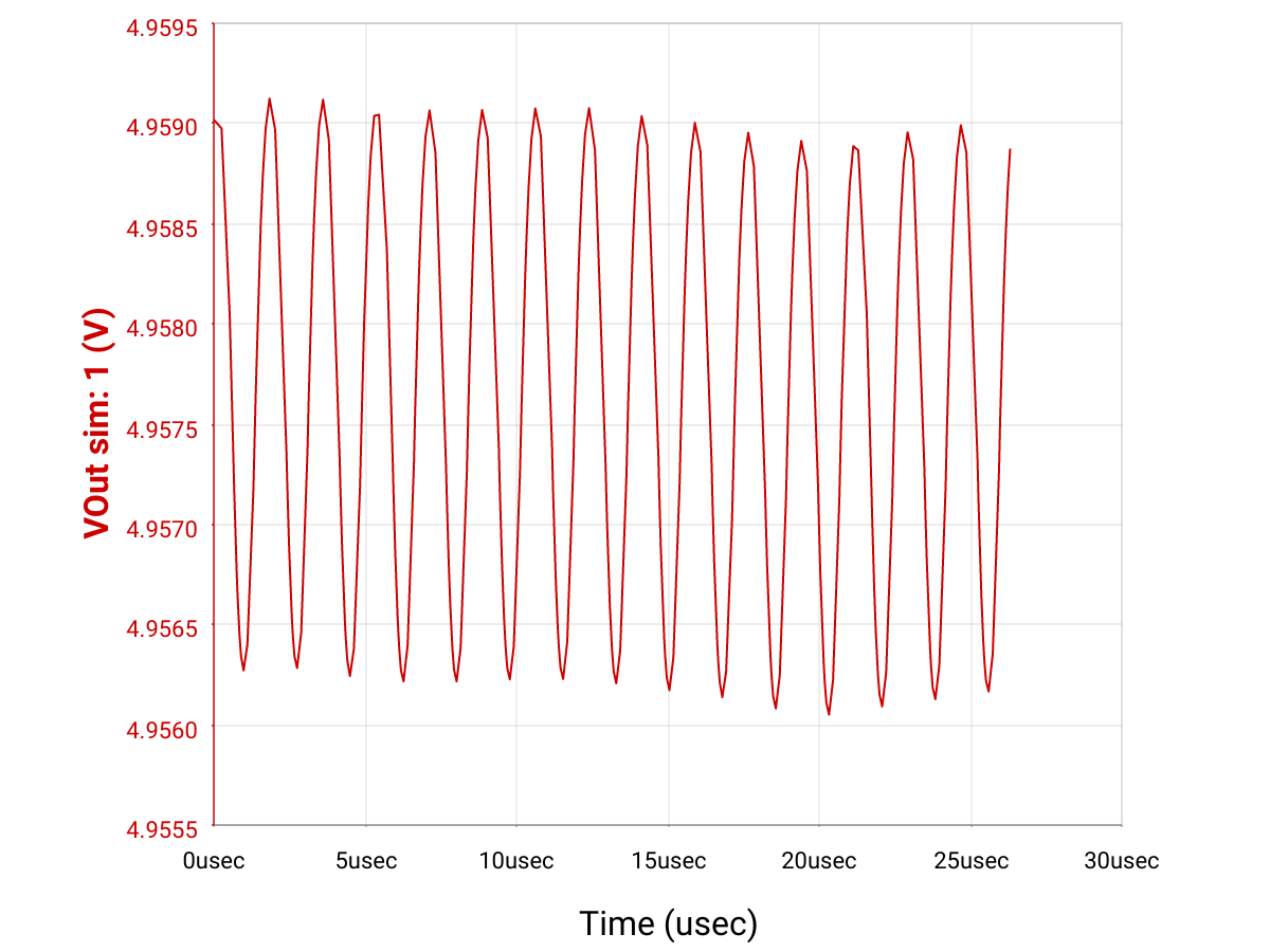
The final buck converter design placed on the ME had two main requirements. The first requirement was that the switching controller IC used needed to be within the JLC part library. The second requirement was that the voltage ripple be small enough for the 5 V output to be a viable power supply to the hall effect current sensor. The voltage ripple can be thought of as the small AC component of the regulator output. For example, the output voltage of a 5 V regulator with 200 mV ripple can be thought of as 5 V +- 200 mV. The hall effect current sensor is operational between 4.5 and 5.5 V, meaning the converter could do a poor job and the sensor could still function. Voltage ripple is not a concern for the 3.3 V rail since it is obtained from a linear LDO, which have smaller ripple voltages. However, buck converters can have near perfect DC outputs as well, depending on the load. If the current draw from the output is steady-state (constant), the switching regulator can quickly lock onto the correct voltage output via the feedback from the output. The circuit used on the ME was tested through simulation to only have 3 mV of ripple at steady state with an average voltage output of 4.96 V, making it more than suitable to power the hall effect sensor and LDO to provide a 3.3 V rail to the MCU. The design and simulation process for the buck converter circuit was carried out using the TI WEBENCH Power Designer. Webench is a web based tool that can generate buck and boost converter designs based off of user specifications. In the case of the ME, I specified that the buck design should allow inputs between 11 and 15 V. The input voltage is designed to accommodate the battery of the formula car should the ME ever be employed as a current sensing device on the vehicle. Two additional specifications for the design is that up to 1 A can be drawn from the output and a filter was used in Webench to target a switching controller that JLCPCB carries for assembly. The figures below are the circuit diagram generated by TI Webench and the steady state simulation plot of voltage output over time.
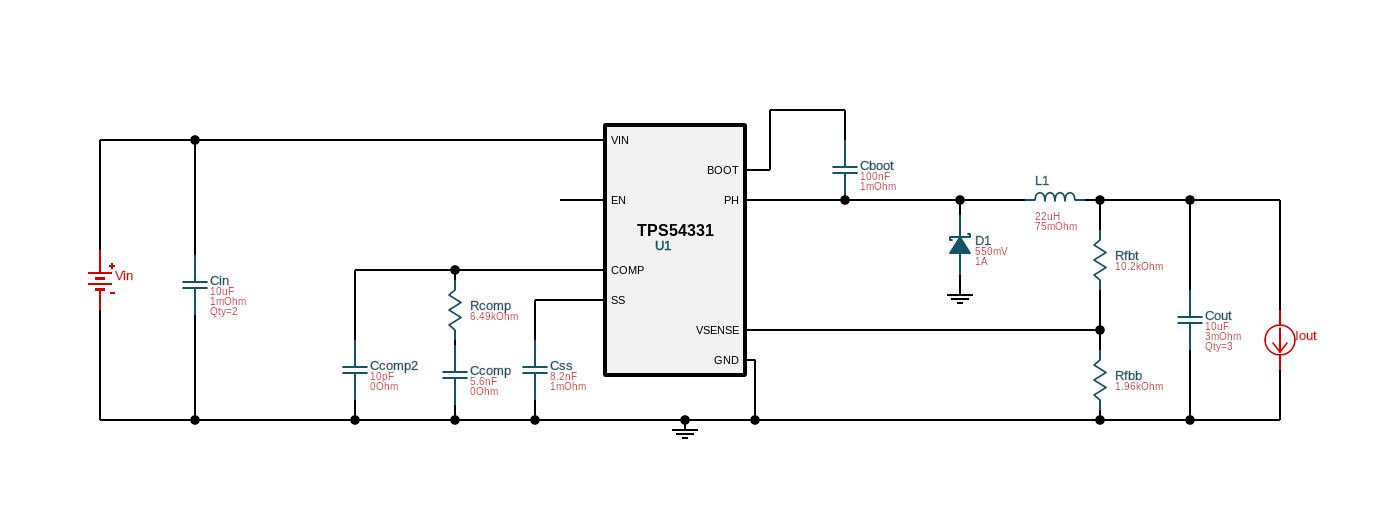
The TI Webench software provides a great starting point for power circuit design, but it is not perfect. I have seen the software provide strange outputs for certain regulator specifications such as capacitors that are multiple farads in size and cannot physically be implemented on a PCB. Thus, it is of utmost importance to consult the datasheet in these cases and tweak the output to a more practical configuration. It should also be noted that the generated designs do not handle the wiring of the regulator enable pins if they exist. In the case of the TPS54331 used on the ME, the regulator will be enabled automatically with the pin left floating, but can also be connected to a voltage divider to program an undervoltage lockout. Undervoltage is a case where the input voltage to the regulator is too low to properly produce the correct output, which in our case is 11 V. The voltage divider connected to the enable pin can ensure that when there is an undervoltage, the regulator will be disabled. The resistors for the voltage divider are selected such that the regulator is disabled when input voltage goes below the 11 V minimum. The final schematic for the buck converter in Altium can be seen in the Project Viewer section of the post in the Buck.SchDoc file. When specifying the voltage divider, I made use of TI’s datasheet which provided formulas to calculate the resistor values found on page 11. These formulas differed slightly from normal voltage divider calculations due to some specific current requirements and pull resistors already present and internal to the device.
LDO Circuit
Connected to the buck regulator output is a low drop out linear regulator used to provide a 3.3 V power rail to the STM32 MCU on the ME. As mentioned in the buck converter section above, a linear regulator is much more suitable to the small voltage drop from 5 to 3.3 V since less heat will result from the 1.7 V drop compared to linear regulation of 12 to 5 V. Moreover, the implementation of an LDO is far easier on the PCB layout side using less parts and space. The LDO circuit can be found in the Project Viewer section in the LDO.SchDoc file. Note that the ME employs a multi-sheet schematic design. If you would like to view the interconnection between the LDO, buck regulator and status LEDs, it can be found in Power.SchDoc.
MCU Circuit
The MCU used on the ME is an
STM32F446RE.
I selected this MCU as it has two built-in CAN controllers and is used on the
Nucleo F446RE development board from STM. Selecting the same MCU as on the
development is useful as it makes code completely portable between the Nucleo
and ME. Additionally, software support for Arduino libraries that STM has
provided on the Nucleo board can also be taken advantage of on the ME. The MCU
is powered by the 3.3 V output of the LDO circuit. Each voltage input is
decoupled with a 100 nF capacitor. Additional bulk capacitors are also employed
as specified in the MCU’s
datasheet. The
BOOT0 pin is also pulled down to ground to configure the MCU to boot up from
flash memory. In order to obtain smooth firmware development experience with the
ME, compatibility with the debugger I designed was implemented.
Thus, I broke out a USART connection and SWD debug lines to go to the debugger.
The SWD and USART pin numbers were collected from the datasheet. In the case of
the USART, I selected USART2 since the nucleo board also connected USART2 to its
integrated debugger. As expected, when using the Serial Arduino library with
the Nucleo board, it automatically maps to USART2. Thus, by using USART2 on the
ME, we ensure better ease of use and compatibility with the Arduino hardware
abstraction layer for which team members are most familiar. Moreover, the Nucleo
development board uses an 8 Mhz crystal to produce a maximum 180 Mhz system
clock via various PLLs inside the MCU. The Mock ECU also uses a 8 Mhz clock
input so that the same startup code used for the Nucleo yields the same system
clock on the Mock ECU. In addition to the debug circuitry, the MCU is also
fitted with two status LEDs connected to GPIO pins. The remaining connections to
the MCU are Altium ports which link to the CAN, current sensing and power
schematics.
Current Monitor
The current sensing capability of the ME is implemented using a hall effect sensor. The sensor output is a voltage which varies with current through the input terminals of the device. The sensor used is the ACS712ELCTR-20A-T. Hall effect sensors work by sensing the magnetic field produced by a current carrying wire and deriving the current from the magnitude of the magnetic field. As a result, the hall effect sensor has the advantage of not needing the current sense resistors required in amplifier based solutions. For additional information on how hall effect and other types of current sensors function, check out this resource.
The current sensor is configured to monitor the 12 V rail of the ME. Thus, the
input voltage is directed through the current sensor and to the board’s 12 V
output connector. In order to perform an accurate power calculation with a
varying input voltage, the 12 V input is connected to an ADC input of the MCU.
However, we cannot sample a 12 V value directly without frying our MCU which can
only handle up to 3.6 V inputs. The problem is resolved using a voltage divider,
which maps the 12 V input voltage to a 0 - 3.3 V range. The voltage divider is
found in the Power.SchDoc file within the Project Viewer section of this post.
Using the ADC of the MCU, we can sample the voltage from the voltage divider and
back substitute accordingly to obtain the source voltage that would’ve yielded
the divider output sampled. Voltage divider formulas without loading can be used
as the ADC input of the MCU should provide such a large input resistance that
any resulting deviation in the divider output voltage would be negligible.
Obtaining the current reading from the sensor is a similar process. Since the
sensor operates at the 5 V logic level, a voltage is employed in the same manner
to map to a value between 0 and 3.3 V for the ADC of the MCU. The output voltage
of the sensor increases linearly with current. However, 0 current does not mean
0 voltage. The
datasheet
defines the zero current output voltage as VCC x 0.5, which is approximately
2.5 V for the 5 V chip supply voltage. The characteristic performance plots
indicate that the linear relation between current and output voltage is such
that for every 1 A increase in current, the voltage goes up by a 1/6 V. This
math can be implemented in software to derive the current from the ADC’s voltage
reading. It should be noted that the voltage read must first be adjusted based
off the voltage divider. The final power calculation can be performed by simply
computing P=VI using the input voltage reading and calculated current value.
CAN Circuitry
CAN bus is implemented on the ME using two CAN transceivers corresponding to the two CAN controllers available on the MCU. The CAN circuit is located in CAN.SchDoc within the Project Viewer section. The transceiver circuit is identical to the circuit that was tested and working in the CT Project with the added benefit of using parts in the JLCPCB library. The transceivers are connected to the broader circuit using Altium’s harness feature which groups multiple nets and allows you to connect them to a single port.
Project Viewer
Embedded below is the Altium project view of the ME project. The embedded viewer contains all the schematics that constitute the multi-sheet design as well as the PCB layout, BOM and 3D renders. The complete Altium CAD files can be found here.
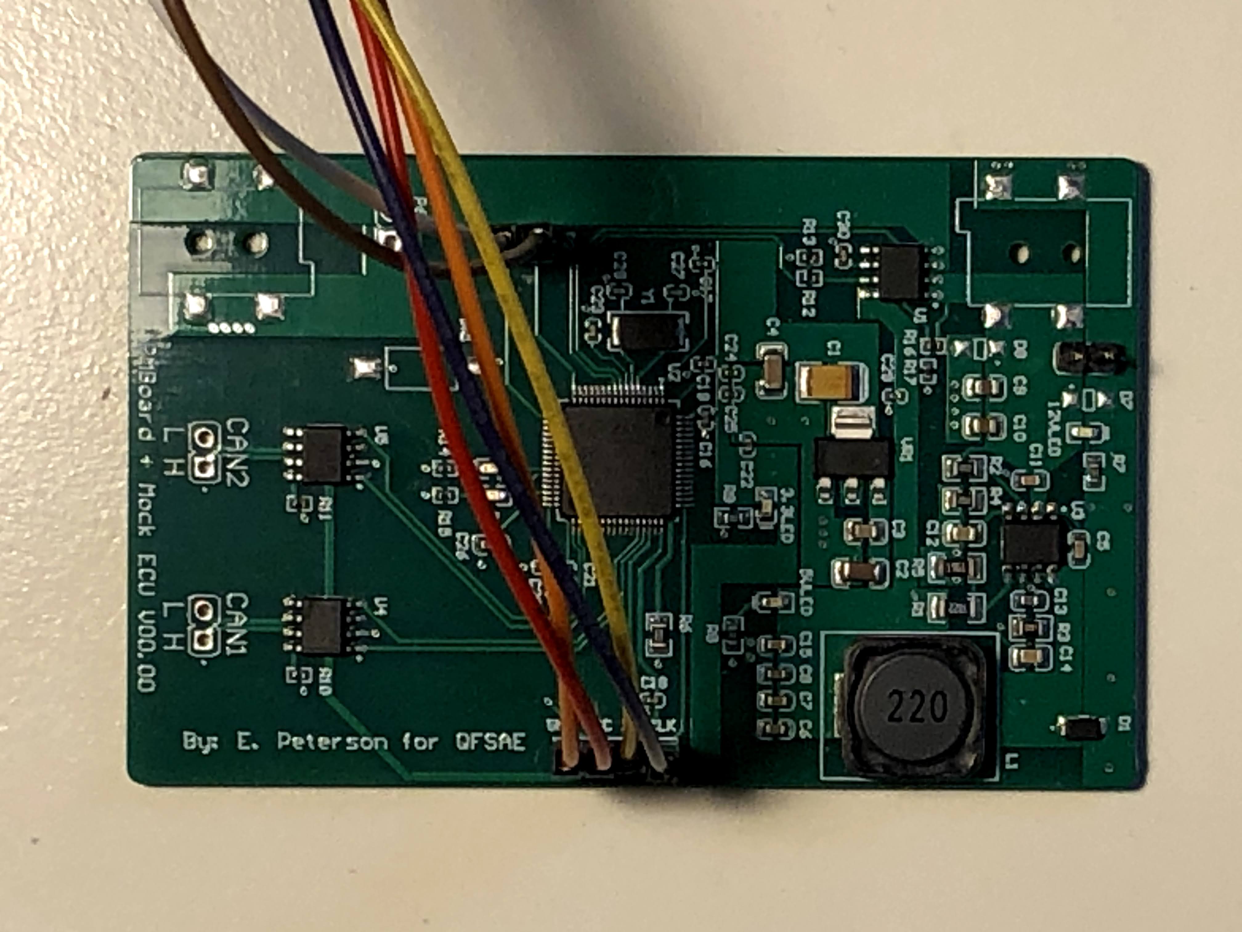
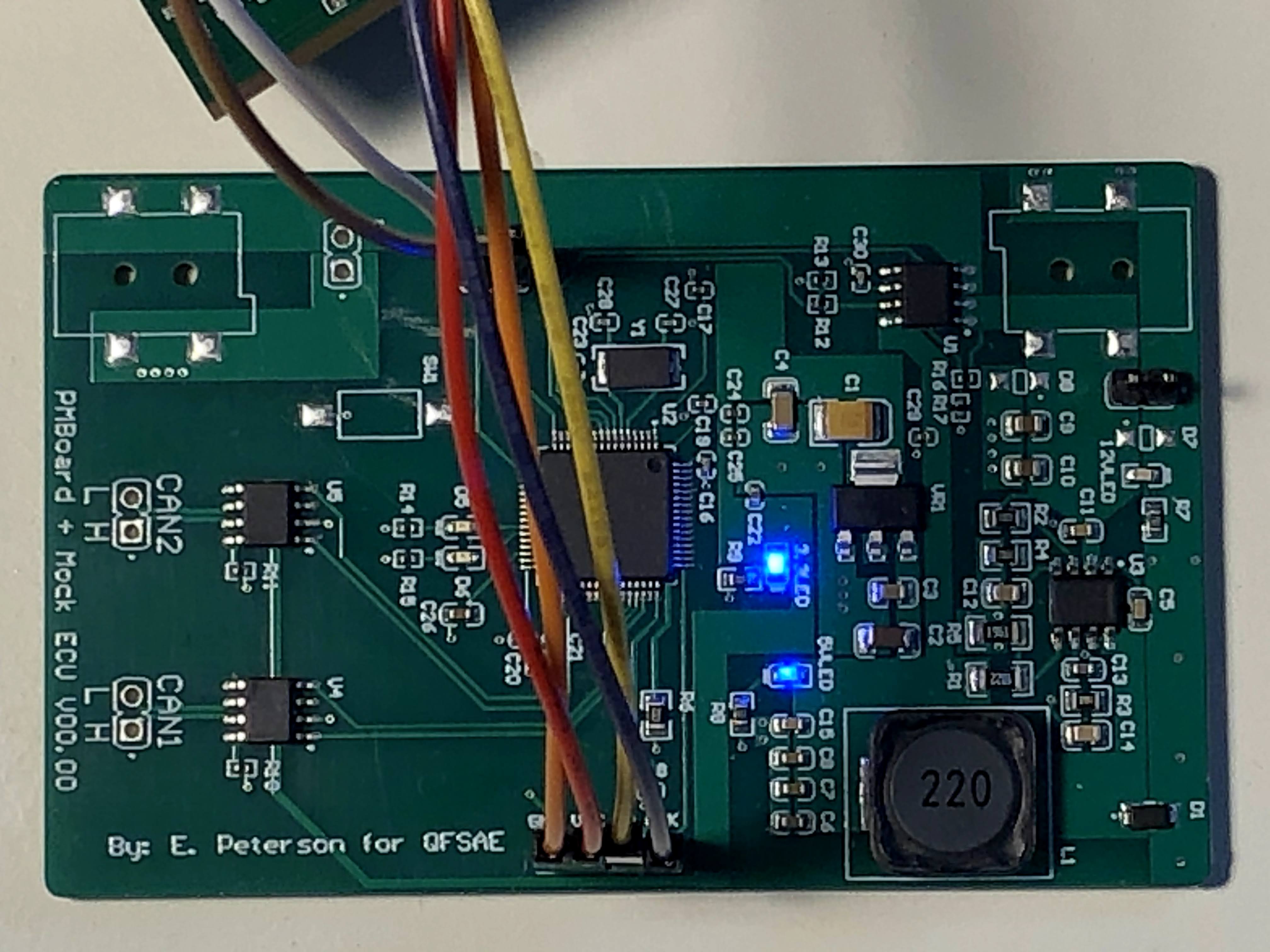
Given below is a photo of the PCB powered up and running. As in past posts, there are some small tweaks I have made to the layout in Altium since receiving the first batch of prototypes. I swapped the inductor for one that is physically smaller and for which it is easier to find suppliers. I also added some additional silk screen for the USART and voltage output headers. The only schematic change is the addition of CAN termination resistors as convenience for the user, so that they are not needed externally.
Manufacturing
The original intention for the ME was to manufacture through JLCPCB’s SMT assembly service. However, the STM32F446RE MCU I selected was not in stock at the time I was looking to order. Due to impatience, I opted to use PCBWAY for both fabrication and assembly. Unlike JLCPCB, PCBWAY will order any part of the user’s choice so long as it is within their assembly capability. Overall, the ordering process was similar to JLCPCB, involving the submission of the BOM, pick and place, and gerber files to PCBWAY’s web UI. The pricing was higher than that of JLCPCB, likely due to the open ended parts selection. However, PCBWAY is still far cheaper than the alternatives I have seen to date.
Software and Board Bring Up
The process of testing the prototypes went smoothly. The assembly quality from PCBWAY was consistently strong with no issues on any of the 5 boards I received. The testing I completed for each board can be divided into 4 categories; power up, debugging, current sensing and CAN. The sub headings below describe how each test was carried out.
Power Up
Power up testing was carried in two separate tests. The first was testing the buck converter by connecting a 12 V DC power supply. As expected, the buck converter output was 5 V, which was successfully converted to 3.3 V by the LDO, thus allowing the MCU to power up properly. The second test was powering the MCU directly through the debugger using the VCC input pin on the debug header, which also powered up the MCU correctly. It was also verified that the ripple voltage matched simulation data for the buck converter’s output under an artificial steady state load (ie. a resistor).
Debugging
Fully testing the compatibility of the ME with my debugger involved testing that
USART passthrough, gdb debugging and program flashing were all functional. The
USART and flash tests were carried out by uploading a hello world program to the
board, which was successful. The debug test was carried out using the gdb-multiarch
command line tool and attaching to the target, which allowed me to walk through
the same hello world program step by step. In this stage, I also verified that
the appropriate registers for external oscillator use had been configured and
the expected 8 Mhz clock was present from the oscillator using an oscilloscope.
Current Sensor
Current sensor testing was carried out by verifying that the sensor is behaving as expected using voltage probes without writing any software. As discussed in the earlier current sensor section, the zero current voltage output is 2.5 V. Probing the sensor output without any load connected read as 2.5 V on the DMM and increased with resistive loads connected, indicating that the circuit is correct.
CAN
CAN testing was carried out by connecting the ME to a standard Arduino CAN bus shield mounted on an Uno. The CAN code that ran on the ME can be found here on the Queen’s Formula GitHub repository. I checked for message send and receive to the ME over both CAN controllers, which were working. Further work will be done here on making a better software abstraction for CAN.
Demo
Embedded below is demo of the ME connected to a debugger running a simple blink / hello world program.
Conclusion
Overall, the ME project has been a great success in tying together the STM32 knowledge I have obtained into a practical development board. The ME board will serve as a basis for the a future project which will integrate the debugger for a single fully featured development platform. Since bringing up the ME board, I have been using it for all my software development. I will be covering the my full exploration into various software development workflows and environments on the ME in a future “A Better Arduino” series post.