JLCPCB Assembly: A CAN Transceiver Breakout
Introduction
After soldering the PDP project, it became clear to me that some of the devices used on that PCB were becoming impractical to solder by hand. Specifically, the 208 pin QFP package of the MCU required a digital microscope to properly align on the pads of the PCB. Knowing that I will be spending more time with these less friendly packages such as QFPs, QFNs and BGAs, I started to look into having my bare boards assembled. In the PDP project, the bare boards were ordered from JLCPCB, which is also an assembly service. The assembly service has a few key limitations which keeps its cost low. The most important of these limitations is that JLCPCB only assembles parts that they have in stock in a library that is searchable on their website. The full list of assembly constraints is listed below.
- All surface mount components must be on one side of the board
- Through hole parts will not be soldered
- Board must be at least 20 x 20 mm
- The components must be from the JLCPCB parts that are kept in stock at their manufacturing facility.
- The part being populated on the board must be within the size and clearance constraints given by JLC PCB (any part in their library will meet requirements).
In addition to the assembly requirements above, JLCPCB has some manufacturing limitations for bare boards in regard to clearances, hole size etc. Those manufacturing limitations and capabilities can be found here.
Design
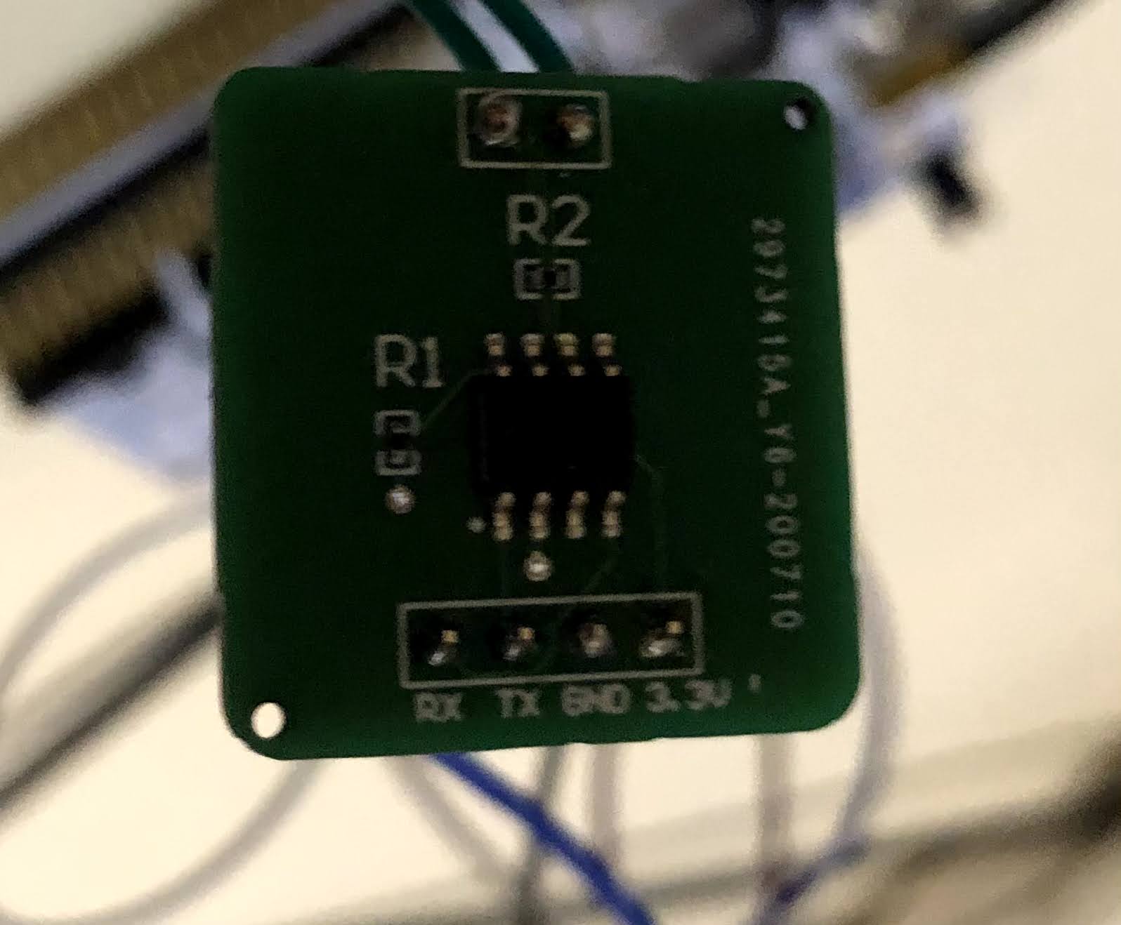
From a design perspective, the CAN Transceiver board (hereby referred to as “CT”) is trivial. The PCB simply breaks out power and data connections (a total of 4 wires) of the SN65HVD230DR SMD Transceiver IC. The CT also has the transceiver pre-configured with a CAN bus termination resistor, which can be de-soldered if it is not needed. The Transceiver chip takes the single ended Rx and Tx signals from the CAN controller inside the MCU and converts it to a differential output to broadcast or receive messages from the bus. If you are unfamiliar with CAN bus and its network topology, check out the CAN bus introduction guide I wrote for the Queen’s Formula team here. Section 1 covers the basics of CAN from both software and hardware implementation perspectives. If you are interested in the the use of differential amplification to produce the differential signal and the benefits of differential signalling in general, check out a brief research report that myself and one of my classmates wrote regarding this subject. The schematic and layout of the CT are given in the following sections.
Schematic
Layout
Manufacturing Files & Altium Configuration
As a result of ordering a fully assembled PCB, the manufacturer requires more information than just gerber files. Specifically, JLC PCB needs a Bill of Materials (BOM), which is a spreadsheet containing a parts list for the project and the designators (R1, C4, U2, etc.) Additionally, a pick and place file is needed, which tells the pick and place machine where to place each part depending on the designator in the BOM. When ordering the PCB, the JLC PCB website walks the buyer through uploading these files and attempts to automatically match part numbers in the BOM to their own library but it is not always successful. When no match is found automatically, manual matching is required and if there is no match, the component will not be populated on the board. In order to make the production process easier, I made use of some specific features and libraries in Altium. Since JLC PCB will only solder a specific set of parts, it is very helpful to have a library with those parts instead of finding or manually creating schematic symbols and footprints. The Altium library I use can be found here. The library does not have all the parts in the JLC library but saves much of the work of finding the appropriate footprints. To accommodate the manufacturing constraints of different PCB fabricators, Altium has the Design Rule Check (DRC) feature. The design rules define when the check returns errors such as un-routed nets or clearance problems. Setting up design rules that match the capabilities of JLCPCB ensures that JLC PCB will be able to produce the board you design. Fortunately, these rules do not need to be entered manually. There is a repository on GitHub, which has design rule files tailored to JLC PCB. I imported the design rules for a two layer board (since the CT is two layer) by following the tutorial in the Altium documentation. As a final step to streamlining the design process, I added an output job which allows for the generation of the BOM, pick and place and gerbers from one place instead of doing each individually. Documentation on output jobs is here.
Testing
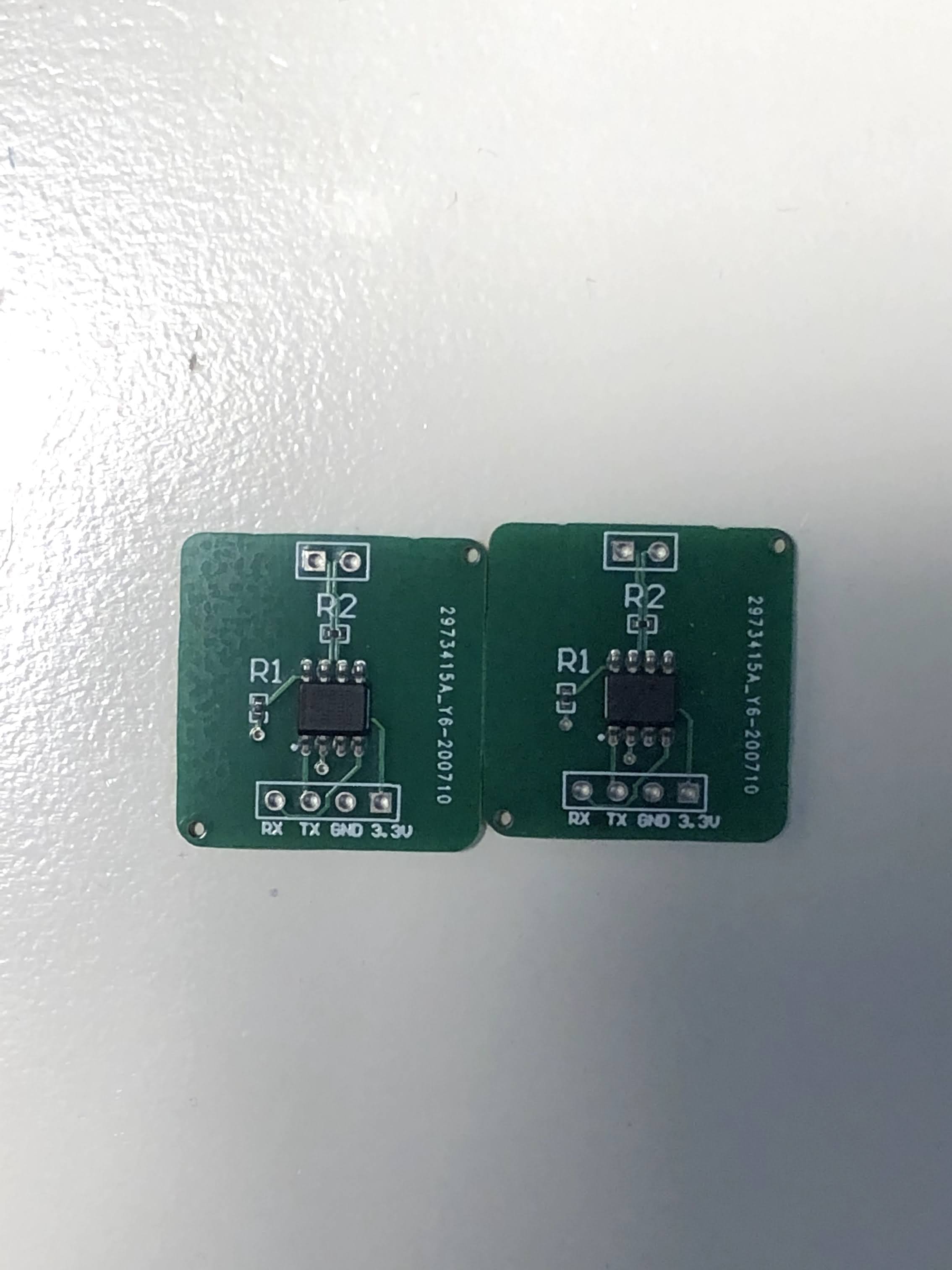
I ordered 5 assembled CT boards, no soldering issues were found on the CT boards. Below is a figure of a pair of assembled boards for reference.
As always, the full design files for the CT project can be found on my GitHub here. The files include the schematic, layout and output job.
Conclusion
Overall, the CT project was a successful exploration into PCB assembly services. Now that I have an Altium workflow set up for JLC PCB, I will continue to employ their assembly service for projects that use parts in their selection.