TeachEE: The FPGA-Based USB Oscilloscope
Introduction
TeachEE (Teach Electrical Engineering) is a USB oscilloscope implemented with an FPGA, custom PCB, and accompanying desktop application. TeachEE was my capstone project and served as the culmination of my four years in Computer Engineering at Queen’s. Despite the branding, there was no commercial intention behind TeachEE as similar cheap USB-based instruments already exist for students. Instead, the purpose of the project was to showcase the “full stack” of skills learned in Computer Engineering.
The project gave me the opportunity the build a complete product from the hardware to the software. TeachEE allowed me to make use of the skills I had learned in my degree and internships:
- Electrical and PCB Design
- Digital Design and Hardware Description Languages (HDLs)
- Knowledge of Signals and Systems, and Digital Signal Processing (DSP)
- Networking and basic communication protocols
- Systems Level Programming
The broad scope of the project required expertise in multiple disciplines within Electrical and Computer Engineering. The benefit of the large scope was that each group member (Eric Yang, Ethan Peterson, Timothy Morland, John Giorshev) could find an area of the project with technical work that interested them.
I took on the hardware design and FPGA firmware as this best aligned with my career background and interests. Eric developed the desktop application for TeachEE, which would display the waveforms sampled by the hardware. The desktop program also allowed for triggering functionality, Fast Fourier Transforms (FFTs), and other basic functions expected of an oscilloscope.
Tim and John took ownership of the signal generator used for TeachEE demos in presentations and competitions. The signal generator utilized the Digital to Analog Converter (DAC) of an Arduino Due to generate arbitrary waveforms to showcase the features of TeachEE. The signal generator used a joystick input to modulate frequency, amplitude, and phase of a signal.
- The overall TeachEE GitHub repository can be found here.
Given below is a copy of the fully detailed technical report provided to the university at the end of the project. This post is a shortened summary of this report.
Hardware Design
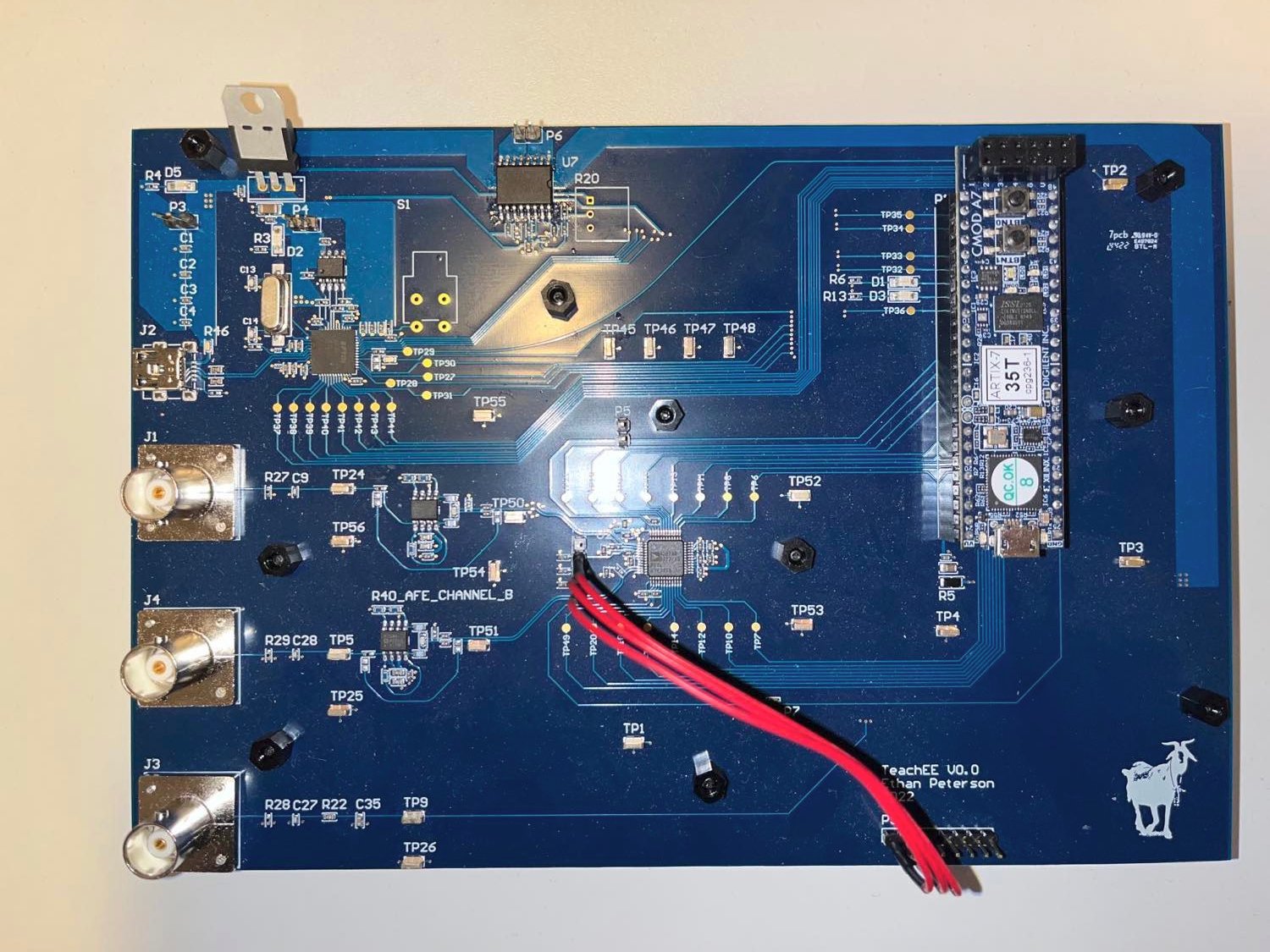
The first step in developing TeachEE was designing the hardware. Three boards were fabricated so multiple group members could do development work concurrently. The primary functional components are listed below.
- FTDI232H in parallel mode for USB communication with the computer.
- AD9288 dual-channel 40MSPS 8-bit ADC.
- AD8138 Differential Amplifier. (Used for analog front-end signal clamping and conversion)
- ACS720 Hall-effect Current Sensor
- CMOD A7 35T FPGA Breakout Board.
For a full BOM and schematic review, please see section 2.1 of the full report linked in the introduction section.
System Design and Block Diagram
Given below is a system block diagram for the TeachEE PCB.
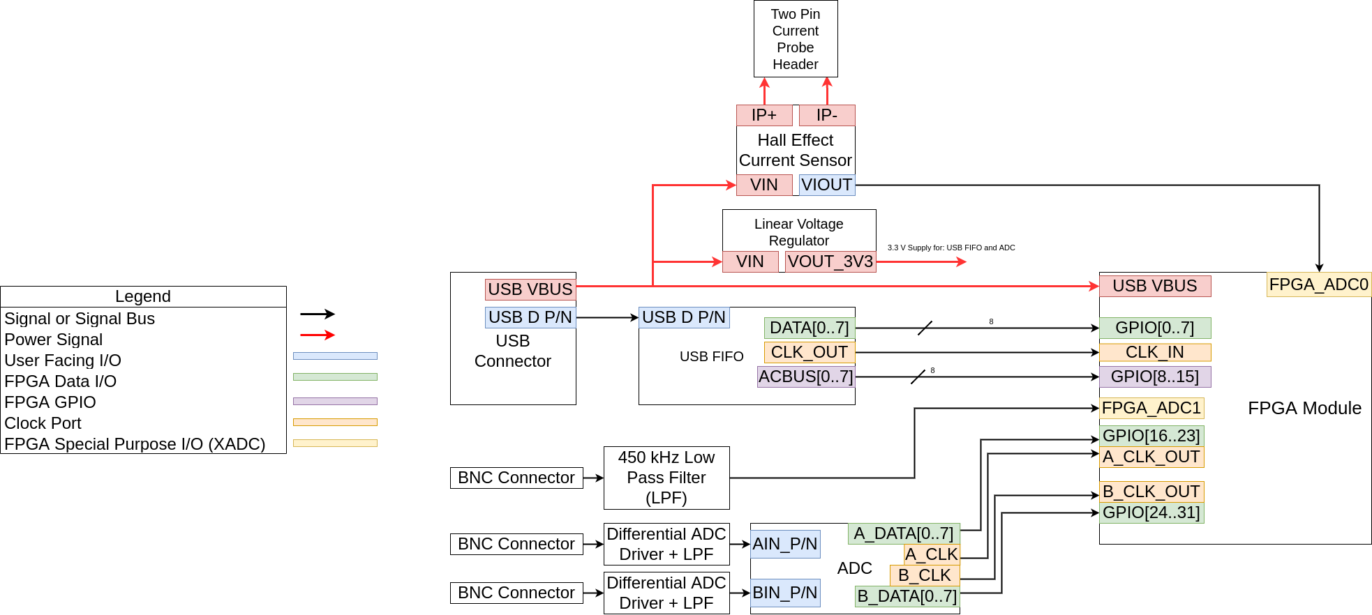
At a high level, the FPGA is responsible for consuming voltage and current samples from three voltage channels and one current monitoring channel. Specifications for each channel are listed below.
- 2x 40 MSPS 8-bit ADC voltage channels
- 1 MSPS 16-bit ADC low-speed voltage channel
- 1 MSPS 16-bit ADC current monitoring channel
Voltage and Current Channels
The FPGA’s internal ADC is used for one of the voltage channels and the current monitoring channel. These channels are limited to 1 MSPS while the external ADC can produce up to 40 MSPS. The slower 1MSPS channels were not initially planned but are “free” to add since the FPGA had a built-in ADC of its own.
Each voltage channel has a Low Pass Filter (LPF) on its input to clamp signals to an acceptable frequency based on the Nyquist Theorem. Additionally, the two high-speed voltage channels connected to the AD9288 40 MSPS ADC have a differential amplifier on the input, which is used to convert the single-ended signal to a differential signal that the ADC can sample. The FPGA is responsible for generating the sampling clock to the high-speed ADC. 40 MSPS is the maximum rate, but any speed can be chosen.
Power Distribution
The board is fully powered by USB which imposes a 5Vx1A (5W) power limit on the PCB. In practice, the PCBA rarely draws current in excess of 100mA. An LDO is used to produce a 3.3V internal power domain.
USB Communication
In order to leverage maximum USB transfer speeds, the full parallel interface of the FT232H USB FIFO is wired to the FPGA. In this configuration, the FT232H generates a 60 MHz clock used to align the 8-bit parallel bus. The FPGA’s internal state machine aligns to this clock and allows the system to transfer a byte of data in each 60 MHz clock cycle. This is known as the “Synchronous Mode” for FT232H. The Synchronous mode allows the FT232H to utilize the full bandwidth available on a USB2.0 interface. For the purposes of TeachEE, the 480 Mbps bandwidth of USB2.0 was sufficient for transferring samples at the desired speeds.
Altium Project Viewer
Given below is an embedded view of the TeachEE Altium Project.
Schematic Design
The TeachEE hardware had to be designed and fabricated within the span of a single semester to allow time for software and FPGA firmware development. As a result, there was only time for a single manufacturing run of the PCB.
Under these constraints, it was critical that the PCB be easy to debug in the case of hardware issues. To accommodate this, I did the following:
- Test points on all digital signals connected to the FPGA.
- BOM stuff options to bypass the LPFs on all voltage channels.
- BOM stuff options to bypass the differential amplifiers on the high speed ADC circuit.
- Empty pads to allow the high speed ADC to accept a single-ended input.
- Use of an external FPGA module connected through a pin header. The decoupling of the FPGA ensured it could be manually wired if there was a mistake in the PCB pinout.
Layout Design
TeachEE is a four layer PCB. The two external layers are used for signals and power, while the internal layers are ground planes. This stackup was used to achieve optimal signal integrity with high speed signals coming from the ADC and USB FIFO.
The TeachEE is larger than necessary to make space for the debugging features listed in the schematic section. All test points and BOM stuff options are spaced out from one another making them easily accessible by oscilloscope probes. Additionally, the board has several dedicated ground tabs that can be used to minimize ground loop size when debugging higher speed signals on the board.
Luckily, these debugging features were not needed as board bring-up went smoothly. The only error in the hardware was wiring the FT232H output clock to a non-clock-capable pin on the FPGA. This issue was mitigated in firmware by minimizing the size of the 60 MHz FT232H clock domain as much as possible in the FPGA logic fabric. Eventually, the logic was optimized to a point where the synthesized design could still meet timing constraints.
FPGA Firmware Design
The FPGA on TeachEE is responsible for taking samples from the voltage and current channels across multiple clock domains and queuing them for transfer to the desktop application over USB. The FPGA also has to frame the samples into USB packets that can be easily and quickly decoded by the desktop application in order to support the high 40 MSPS sample rate.
Given below is the block diagram describing the FPGA datapath. A full module-by-module breakdown is provided in section 3.2 of the report embedded at the top of the post.
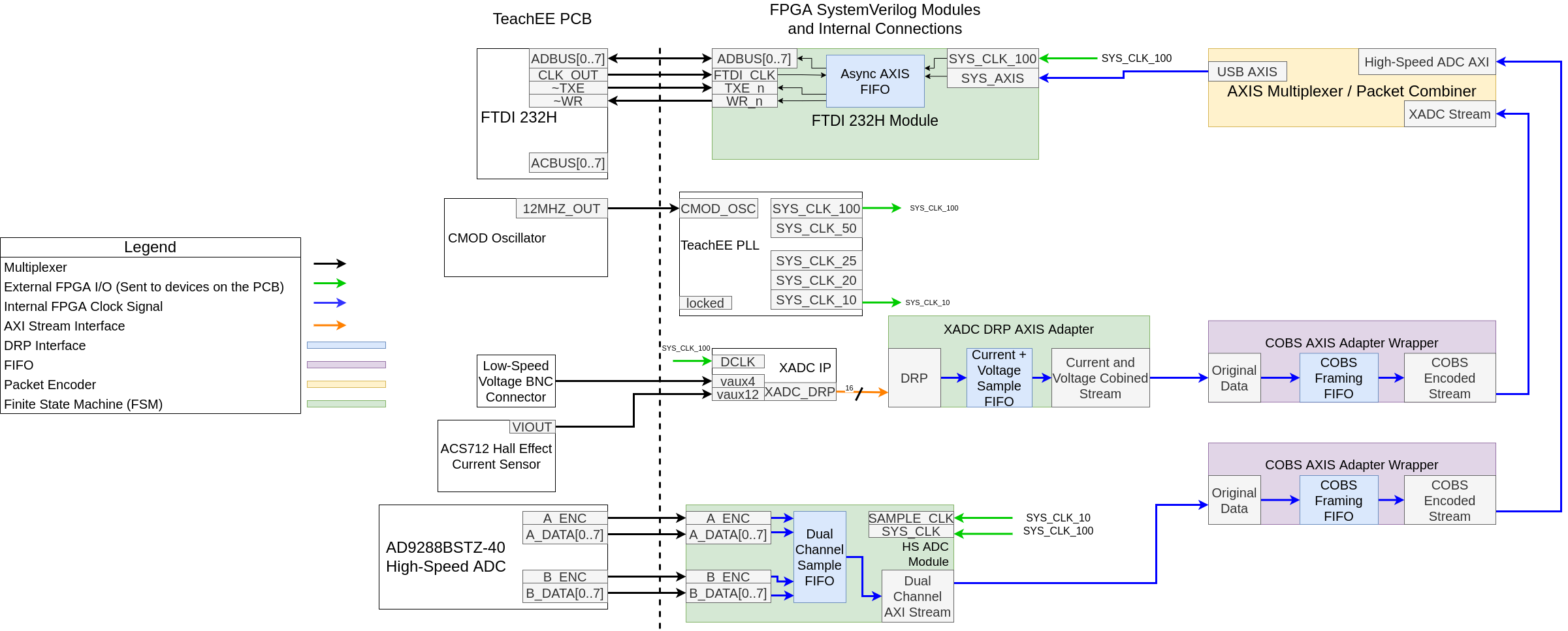
The FPGA has dedicated modules to collect samples from the low and high speed ADCs respectively. Each module outputs the data on an AXI stream. AXI streams are used as a standard interface between modules in the FPGA to make use of various FIFO IPs for queuing samples. These asynchronous FIFOs are used to carry samples across the various clock domains in the datapath until they can be encoded and sent over USB. The FTDI module takes an AXI stream as input and converts it to the parallel interface of the FT232H.
Samples are encoded using Consistent Overhead Byte Stuffing (COBS). However, the FPGA takes an extra step to guarantee a fixed frame size so that the desktop application can have a faster decoding algorithm.
Software Design
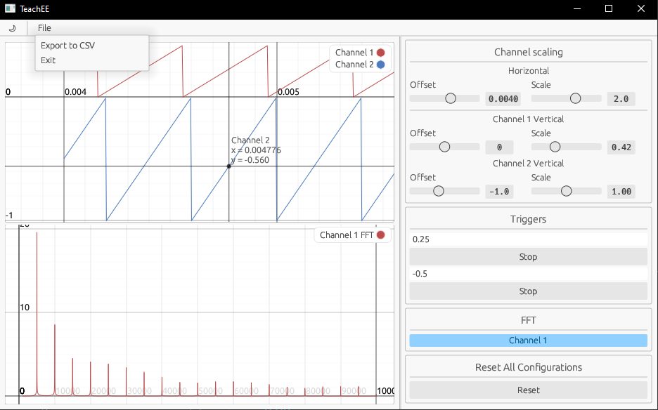
Eric Yang in our capstone group completed the desktop Rust application for TeachEE. This multi-threaded application consumed the multi-channel sample stream from the TeachEE PCB and implemented full oscilloscope functionality, including but not limited to:
- Multi-channel display
- Fast Fourier Transforms
- Triggers
- Time and amplitude scaling
Given below is a sequence diagram for the desktop application and a screenshot of the final UI.
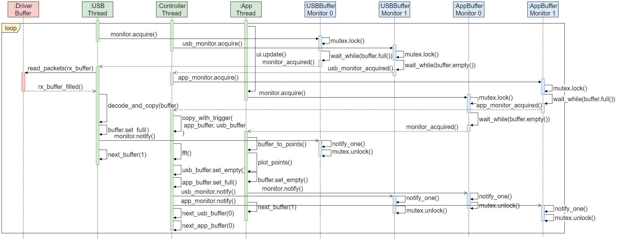
Eric’s full breakdown of the desktop application can be found in section 3.3 of the report.
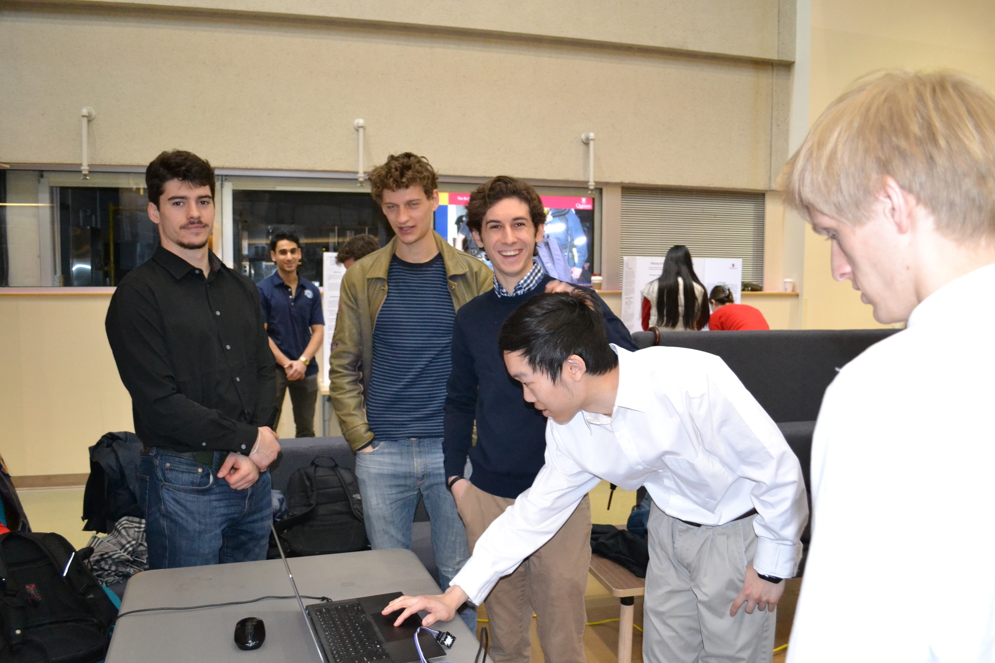
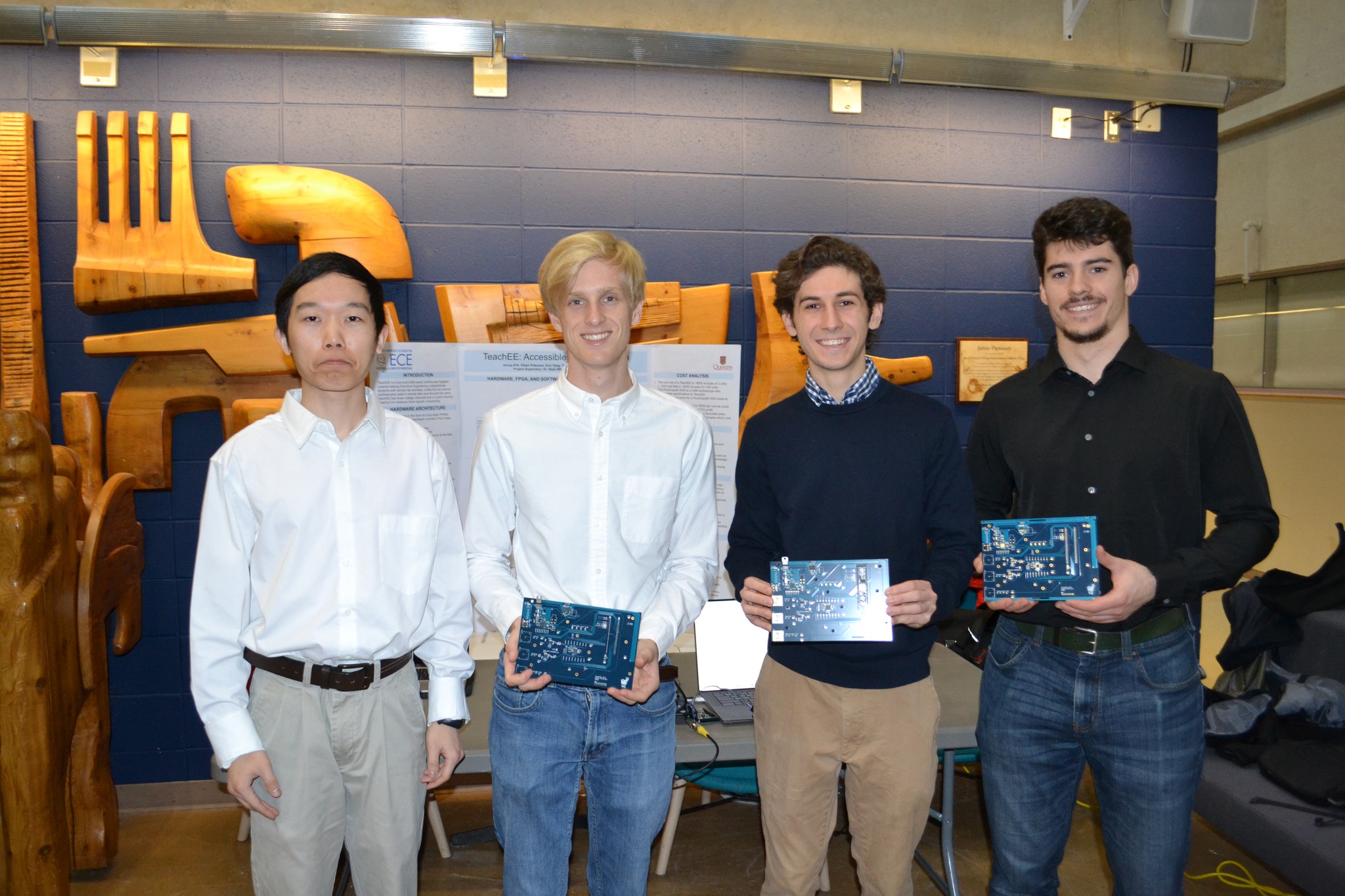
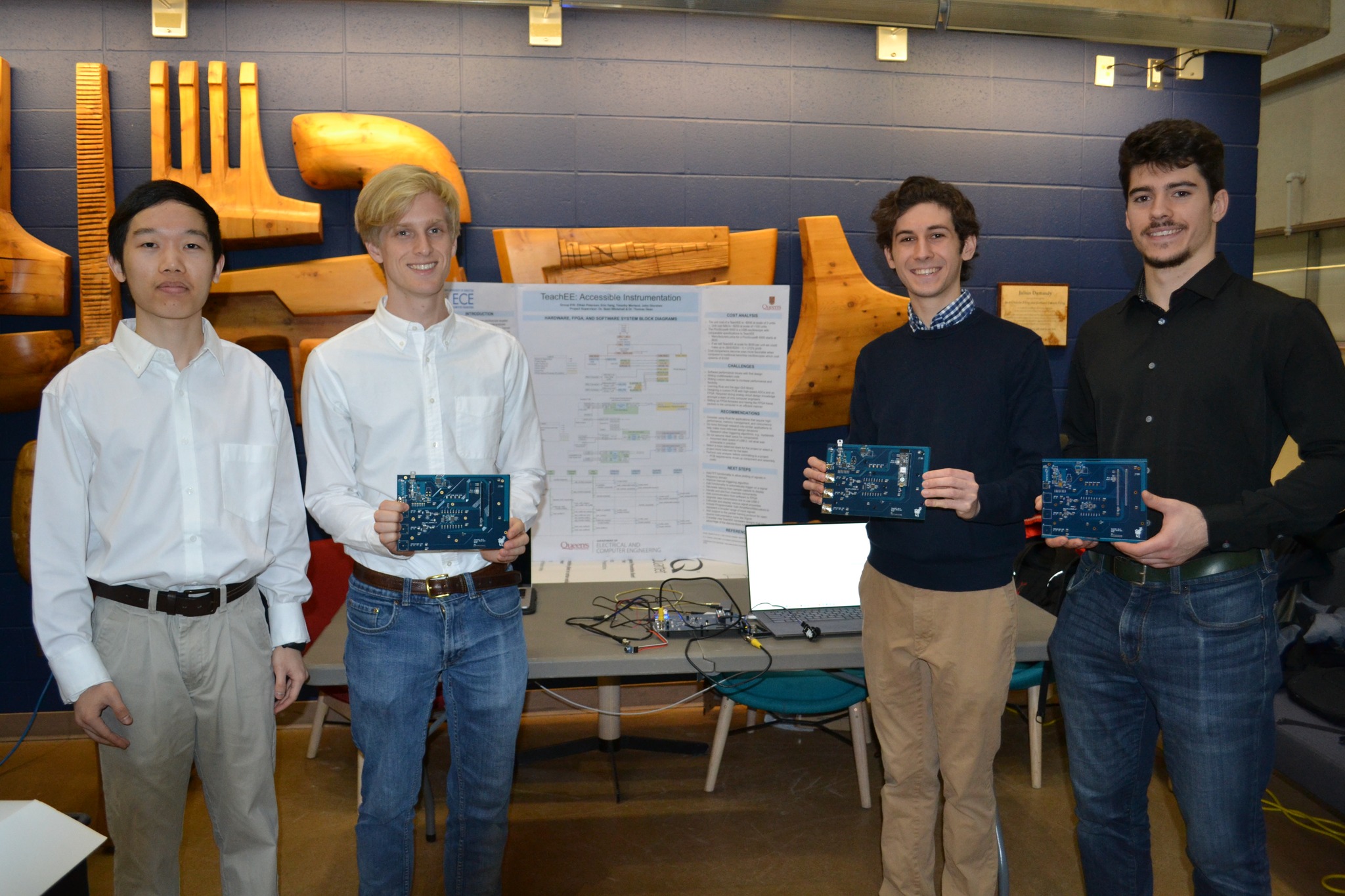
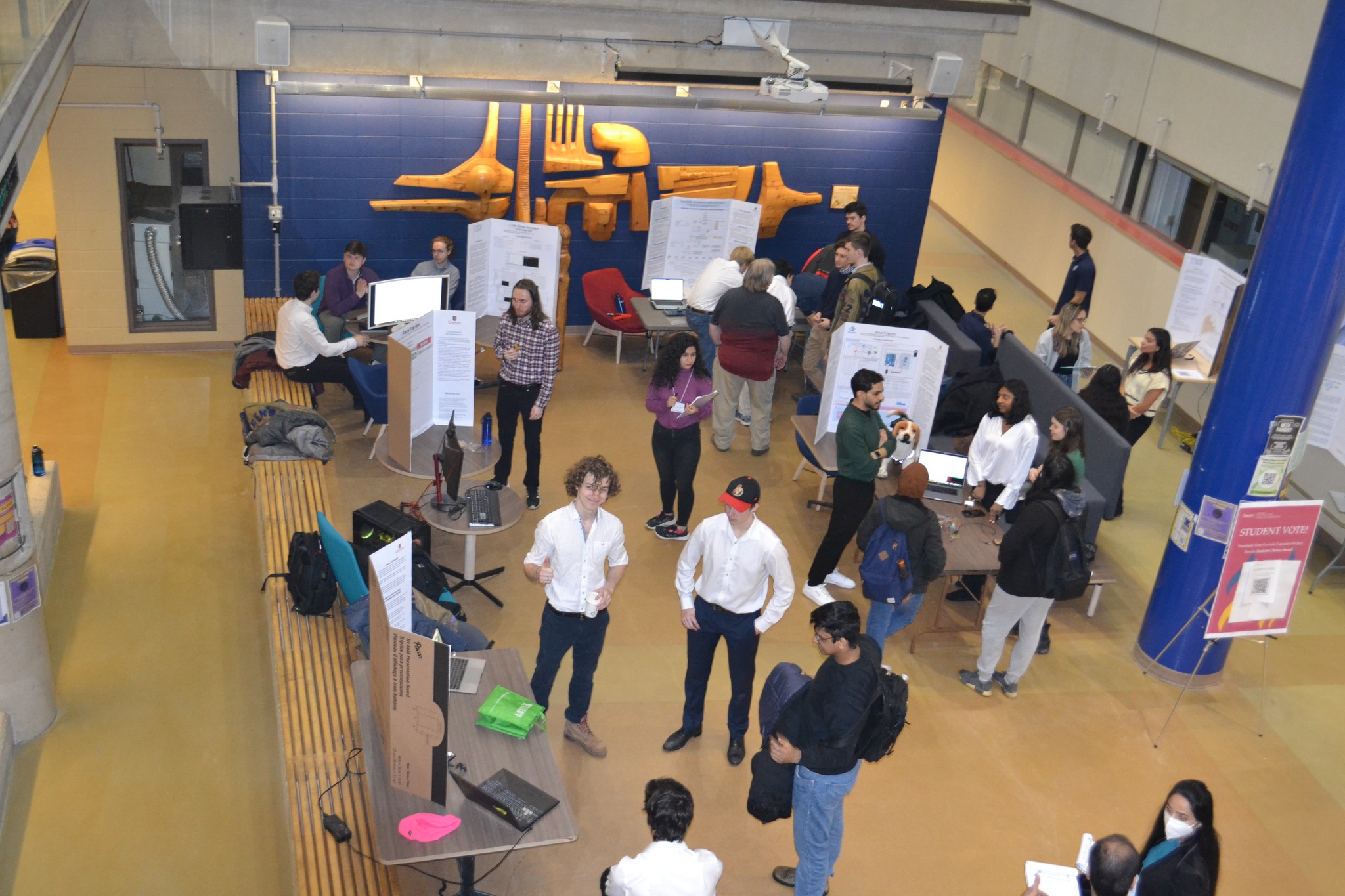
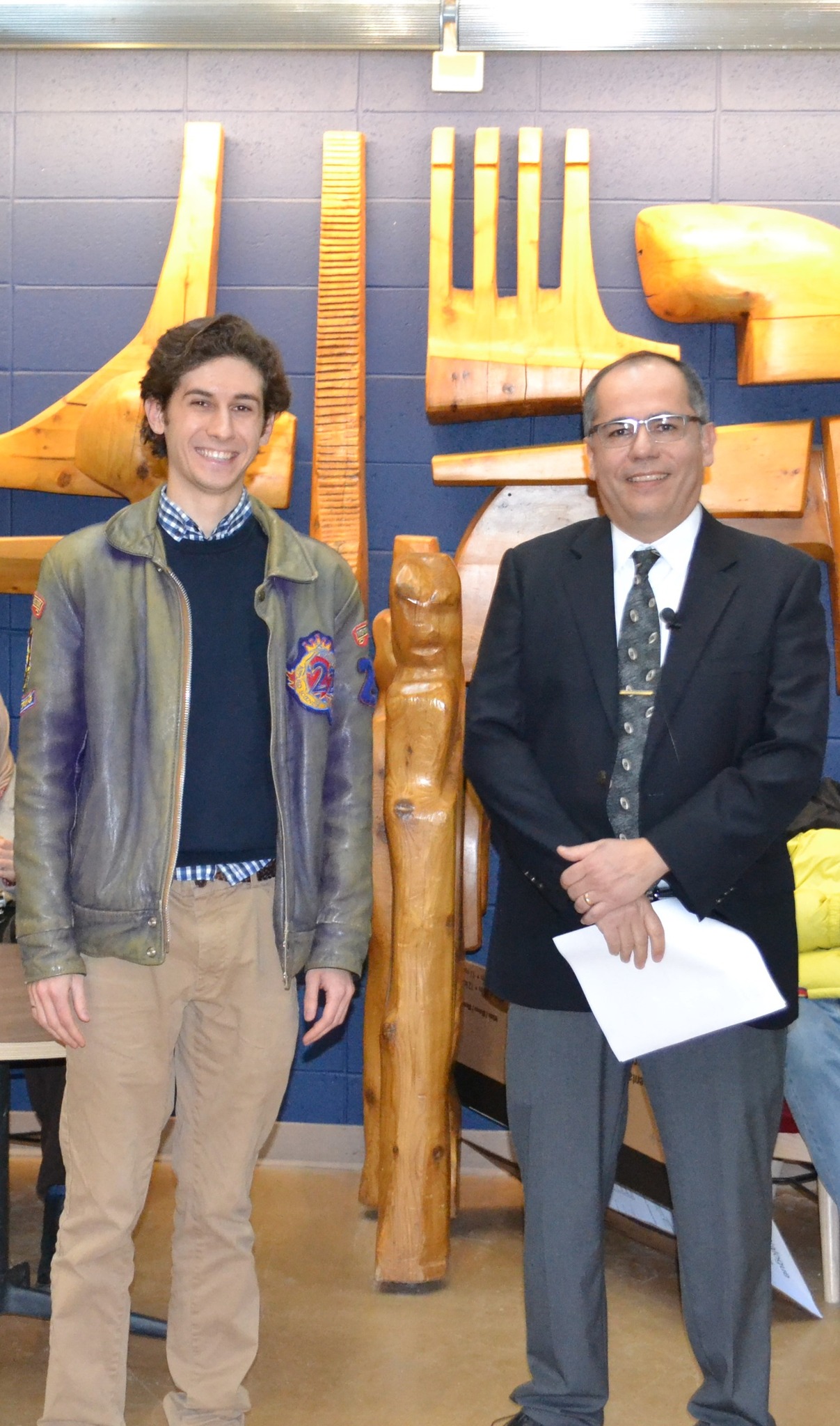
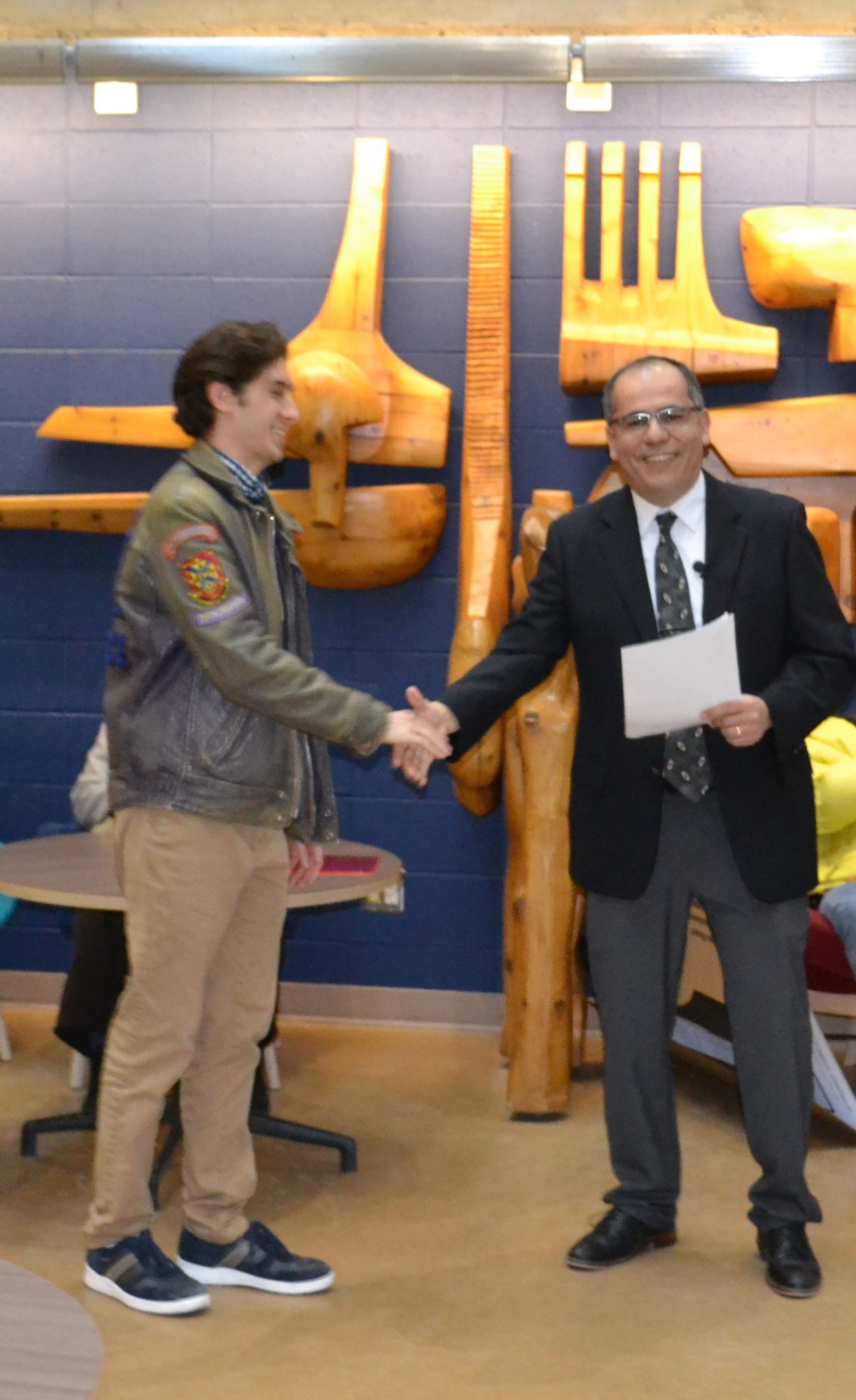
Gallery and Awards
At the end of 2022-2023 school year, TeachEE entered the Queen’s ECE Capstone Competition and won both the department and IEEE awards. TeachEE won first place for both the ECE department and the Kingston Ontario IEEE chapter. Below is a gallery of photos from the capstone showcase.
Conclusion
Overall, TeachEE is a culmination of all my favorite subjects in Electrical and Computer Engineering. Moreover, it was a fantastic way to end my time at Queen’s Computer Engineering. I was thrilled that the project was well-received by the department and that we were able to integrate both hardware and software into a single capstone project.