A Better Arduino: Setting up an STM32 Development Platform (Part 1)
Introduction
The Arduino is easily the most popular embedded development platform available
to hobbyists today. The Arduino libraries provide easy to use abstractions such
as digitalWrite(), analogRead() and more. Moreover, the build and flashing
process onto the Arduino is completely abstracted away by the IDE, making Arduino
an easy starting point. However, there comes a point where Arduino’s various
obfuscations and abstractions of what is happening in the hardware starts to
slow the developer more than it speeds them up. While working on the Queen’s
Formula Racing Team this past year, myself and other
team members ran into this issue repeatedly. Specifically, we were limited by
inconsistencies in the implementations of the Arduino libraries between various
devices such as the Uno or the Teensy. Another troublesome issue was Arduino
libraries that were dependent on hardware specific features and accessed them in
a bare metal fashion instead of working through the existing Arduino hardware
abstractions to make it platform agnostic (ex. a screen library that uses SPI to
drive the display but makes low level calls to the MCU specific SPI interface
instead of using the Arduino SPI library). Some of the issues the team ran into
were Arduino Serial library implementations that did not allow the programmer to
set baud rate explicitly (Teensy), screen driver libraries that did not respect
the chip select line of SPI and interferes with SPI bus ICs used for CAN bus
communications. After long debugging sessions diagnosing these issues, we came
to the conclusion that some of our team projects had enough moving parts
to warrant an upgrade to a custom MCU solution without necessarily employing
Arduinos or compatible devices such as Teensy.
By not tying the team directly to Arduino, we can select MCUs that are more directly suited to automotive applications and our specific use cases. The main requirements for a new MCU platform were built in CAN bus peripherals and multiple USART peripherals to support print statements and inter-MCU communications over USART. The MCU platform selected was STM32 from ST Microelectronics. STM32 is 32 bit ARM based line of MCUs with various models of different sizes, performance and peripherals. In order to test the viability of STM32, I opted for an MCU that had all the peripherals we needed and selected the STM32F769BIT6. This chip comes in an LQFP-208 package and boasts multiple USARTS, A DSI hardware peripheral and most importantly, three CAN buses. Historically, the team had made use of the CAN Bus Shield from Seeed Studio. The circuit on the shield had to be copied onto the team’s custom PCBs, adding complexity to each design. The CAN peripherals on the STM32 MCU remove the need for this circuit while also opening the opportunity to run multiple CAN buses for higher data throughput without copying the bulky SPI circuit several times over. Moreover, the CAN peripherals on the STM32 support interrupts on message receive, thus allowing the team to abandon the clunky polling based approach used on Arduino. With an MCU selected and tested, I set out to layout the MCU on a custom PCB. It was essential to be able to use STM32 on custom PCBs since most team projects involved boards with highly constrained form factors where placing a standard development board sold by ST on the car would be infeasible.
Designing the Board
The first iteration of this STM32 development platform is affectionately named the Peterson Development Platform (hereby referred to as the PDP). This simple test PCB has the objective of properly powering up the MCU and running basic programs on it, such as blinking an LED. The schematic design of the PDP can be broken into the following three steps:
- Powering the MCU
- Clocking the MCU
- Debug and Programming Access to the MCU
Powering the MCU
Information on powering the MCU can be found in the datasheet. The power up circuit is shown in Figure 25 of the datasheet, which is provided below.
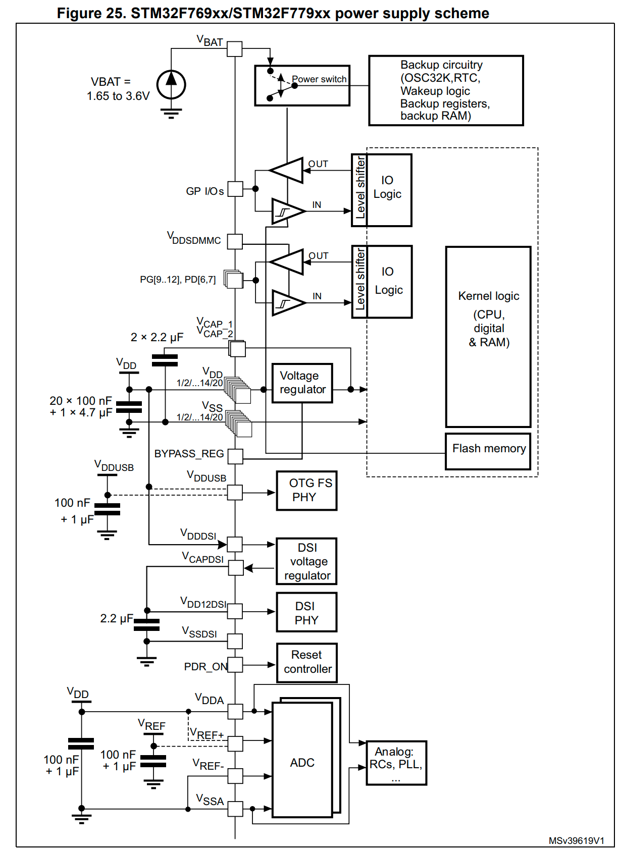
In summary, the MCU has many VDD power input pins which expect a 3.3 V input. The 3.3 V power is provided through an LDO which regulates down from 5 V or through a direct 3.3 V from a debugger connected to a computer. However, as shown in the figure above, the 3.3 V power cannot be directly connected to the MCU and needs various bypass capacitors. Each VDD pin has a 100 nF bypass capacitor connected between 3.3 V and ground. These capacitors are short circuits at AC and open at DC. Thus, the noise on the DC power signal is filtered and as a result the MCU receives a cleaner DC power input. Also shown on the diagram are larger bypass capacitors in the uF range which are employed to compensate for any sudden drops in voltage from the power supply. The LDO circuit and assortment of filter capacitors can be viewed in the Schematic section.
Clocking the MCU
In order to fully utilize this MCU, an external clock is needed. By default, the MCU starts up using the internal RC oscillator which is limited to a 16 Mhz system clock. This speed is too slow to use some peripherals and does not take advantage of the maximum system clock of 216 Mhz. In this case, a crystal oscillator is used with a frequency of 25 Mhz which can yield the full 216 Mhz system clock with the correct register configuration loaded onto the MCU. The correct pins for connection to the crystal are found in the datasheet. In this case, PH0 and PH1 are the pair which were used. In order to obtain stable and accurate oscillation, the correct shoulder capacitor values must be selected to match the crystal. The load capacitors used on this specific crystal are 18 pF. This value was calculated using formulas provided in an application note from ST. The document is for all oscillators in general and provides instructions to calculate shoulder capacitance based on data sheet parameters and whether an external series resistance is needed. It should be noted that the schematic also includes a second oscillator at a frequency of 32.768 kHz. This oscillator is not needed for the operation of the MCU but was instead added in order to use the RTC peripheral and keep track of time. The shoulder capacitors for this oscillator were derived from the formulas in the application note in the same manner as the system clock oscillator.
Debug Access to the MCU
The final step in the schematic design of the PDP was setting up debug access to the MCU in order to flash and test code. The vast majority of STM32 MCU product lines support ST-Link, which is an Serial Wire Debug (SWD) based debug and flash protocol. SWD is a two wire interface with a clock (SWCLK) and data line (SWDIO). Each STM32 that supports ST-Link has default pins mapped to these functions. In the case of this MCU, those pins are PA15 and PA14. The two pins were then broken out on a 4 pin header which added a power input and ground connection in the top left of the schematic. The ground connection is needed for signal integrity so that the debugger and PDP have the same ground reference. The power input also allows the PDP to be powered off a 3.3 V output of the debugger. With the debug header in place, any ST-Link compatible debugger can be used.
Schematic
Below is an interactive schematic viewer. There is a Bill of Materials (BOM) tab which is the parts list for the project.
Layout
Below is an interactive PCB layout viewer for the PDP.
Testing the Board
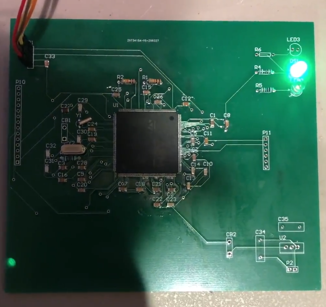
The PDP was ordered via JLC-PCB and hand soldered. After soldering the debug header, the board was ready for testing. Using this ST-Link Debugger from Adafruit, the power LED on the PDP lit up indicating that there are no shorts. The next step was to test the debugger connection using the ST-Link utility. Links to an ST-Link utility for each operating system are listed below.
Using the ST-Link CLI tool, I ran st-info --probe to test the connection,
which indicated that both the programmer and MCU target were found. With the
debugger properly configured, the final step was to write a simple test program
that blinks an LED on the PDP. In order to complete this task in a timely
manner, I utilized the STM32 hardware abstraction layer (HAL) and project / code
generation tool
STM32CubeMX.
STM32CubeMX allows the user to select any STM32 MCU and configure the clocks and
peripherals in a graphical manner. After configuring your MCU, STM32CubeMX will
generate a project with all the initialization code corresponding to your
configuration. Moreover, STM32CubeMX can output multiple project formats from
STM32CubeIDE to a traditional Makefile based project. The ST wiki provides a
tutorial on
setting up a blink program and running it from
STM32CubeIDE.
Instead of selecting a nucleo board as the target, the MCU selector was used to
select the STM32F769BIT6 MCU on the PDP and pin PJ15 was used for the LED
instead of the mapping for the example board. Since the board is connected via
ST-Link, building and running code worked out of the box. The complete code is
available on
GitHub.
A demo of the soldered PDP running the blink program is given below.
Design Files
All of the Altium Designer CAD files are located in this GitHub repository. The repository also includes my other PCB projects that use Altium.
Conclusion
Overall, the PDP is a good first step towards a more fully featured STM32
development platform. However, the PDP is still far from equivalent to the
Arduino with respect to ease of use. Specifically, the project creation project
is more complex and there is no USART or print() capability over USB as there
is with Arduino. The Nucleo development boards manufactured by ST bundle both
debugging and serial over one USB connection. In future posts, we will examine
how to get these features up and running as well as setting up a more easy to
use workflow for writing software.