An FPGA Peripherals Library Written in SystemVerilog
Introduction
After completing the TeachEE project, I began to further explore
FPGAs in my spare time. The result was the
peripherals library. This
library implements a variety of communications peripherals typically found in
microcontrollers on an FPGA. The library is implemented in SystemVerilog and
provides a standardized AXI interfaces for using these protocols on an FPGA.
At the time of writing, I have implemented the following:
My goals behind creating this library were to:
- Improve my FPGA development skillset.
- Design custom state machines to implement many of the peripherals we take for granted on a microcontroller.
- Provide a reference for my own future projects to quickly integrate these protocols in an FPGA development environment.
- Utilize Ethernet and begin taking advantage of high-speed communication protocols (i.e UDP).
This library was made strictly to learn how to implement these protocols at the hardware level. While I have validated all the modules in simulation and on-bench, they are likely not as thorough or capable as some of the other mainstream open source options available. They do serve as a great introduction to these protocols and systems nonetheless.
The Peripherals Repository
The peripherals repository
contains the source modules for each peripherals in addition to VUnit
testbenches, bus functional models (BFMs), and usage examples.
All the modules are regression tested by VUnit testbench. Each testbench is run on every commit using this GitHub Actions job
This GitHub actions infrastructure is taken from my project template here, which was in-turn influenced by the GitLab template from Alex Lao.
Modules
The following subsections provide a brief overview of each peripheral available in the library. All the modules use an AXI stream or AXI Lite interface. Below are some recommended resources for AXI.
UART
The UART peripheral implementation can be found here. The module interface is as-follows:
module uart #(
    parameter TX_FIFO_DEPTH = 32,
    parameter RX_FIFO_DEPTH = 32,

    // Equates to a 115200 bps rate on 100 MHz clock.
    parameter CLKS_PER_BIT = 868
) (

    // asynchronous RX signal
    input var logic rxd,

    output var logic txd,

    axis_interface.Sink tx_stream,
    axis_interface.Source rx_stream
);
Two AXI stream interfaces are used to transmit and receive UART bytes. Both
stream interfaces are connected to a FIFO queue specified by the FIFO_DEPTH
parameters. This allows the parent module to queue bytes for transmit
asynchronously to the underlying UART transmitter and avoid the need to
continuously poll for received bytes.
The FIFOs are wrapped in an axis_interface interface type to group the
relevant AXI stream signals together. The original FIFO module is provided by
the verilog-axis library.
Instead of generating a low-speed clock to send UART data, the
transmitter/receiver state machines use the CLKS_PER_BIT parameter to send
data at the correct baud rate. Using the main high-speed clock and counting
cycles is preferred for the following reasons:
- Full control of when the UART RX line is sampled.
- Avoids creating an additional clock domain and resulting metastability issues.
However, there is still one metastability concern in the UART receiver. Since the RX line is asynchronous to the FPGA clock, it must be synchronized before its data is processed to avoid incorrect sampling and data loss. This synchronization to the FPGA’s clock domain is implemented with a Two-Flip-Flop (2FF) Synchronizer module.
SPI
The peripherals repository implements a simple SPI Master. The SPI module interface definition is as follows:
module spi_master #(
    parameter TRANSFER_WIDTH = 8,

    // default for a 100 MHz clock
    // produces 1 MHz SPI
    parameter CLKS_PER_HALF_BIT = 50,

    parameter CPOL = 0, // sck idle state
    parameter CPHA = 0 // sampling edge (0 for rising, 1 for falling)
) (
    input var logic miso_en,
    spi_interface.Master spi_bus,

    // it is assumed that these two streams share the same clock
    axis_interface.Sink mosi_stream,
    axis_interface.Source miso_stream
);
Parameters
The SPI master module currently only supports fixed data transfer sizes as
defined by the TRANSFER_WIDTH parameter. This simplifies some of the logic
around when the CS line is asserted and de-asserted. However, a future
improvement would be to utilize the tlast signals in the AXI streams to
determine when CS should be asserted. Alternatively, a future iteration could
give full control of the CS line to the parent module for better handling of
multiple nodes on a shared SPI bus.
Similarly to the UART module, the SPI master also uses the main FPGA system
clock and counts cycles to produce a low-speed SPI clock as defined by the
CLKS_PER_HALF_BIT parameter. This approach is beneficial in the SPI use-case
because it allows the module to have precise control over when the MOSI line
transitions and when the MISO line is sampled.
For the MOSI line, it is important to update its state at the correct time relative to the SCK clock signal so that setup and hold times are respected. Similarly, the MISO line must be sampled at the correct time. Another benefit is mitigating FPGA I/O jitter. If the module operated directly on the low-speed SPI SCK clock, this jitter could lead to data integrity issues. The drawback of the cycle counting approach is the increased LUT usage in the FPGA.
The last parameters in the SPI master module are CPOL and CPHA which define
the SPI mode and clock polarity.
Main Interface
The SPI master module interface consists of miso_en, spi_bus, mosi_stream,
and miso_stream. Each signal / interface is summarized below.
miso_enis used to enable and disable miso functionality in the SPI master module. This is useful for SPI devices that do not send data back to the master.spi_busis a SystemVerilog interface grouping all the SPI signals together. (MOSI, MISO, SCK, CS).mosi_streamis an AXI stream where the parent module can load data to be sent to the SPI slave.miso_streamis an AXI stream output that the parent module may use to read data returned by the SPI slave.
Example Usage
The SPI master peripheral was designed to be wrapped by a parent module that contains all the device-specific behavior. While testing the SPI master, I wrote a module which reads and writes registers via SPI on an ADXL345 IMU.
Ethernet and UDP Modules
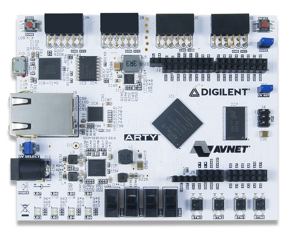
The peripherals repository contains three example ethernet modules. The modules were developed and tested using the DP838X 10/100 ethernet PHY on the ARTY A7 development board:
- UDP Echo
- Echoes received UDP traffic back to the transmitter.
- UDP Transmitter
- Allows the FPGA to transmit data to the host machine with a fixed IP address and port number.
- UDP Receiver
- Allows the FPGA to receive data from a fixed IP address and port number.
All three modules rely on the verilog-ethernet library from Alex Forencich. The library provides the MII interface to the ethernet PHY as well as the IP/UDP stack needed to communicate with a computer and exposes an AXI stream interface for packet data. By combining the MII, ethernet, and UDP modules into a single wrapper, I was able to send/receive UDP via a simple AXI stream interface.
One challenge in configuring these modules was handling the timing constraints on the ethernet PHY. At higher data rates, the FPGA needs to be configured to respect the setup and hold times for the various MII signals and ensure that the correct data is transmitted/received. Before configuring the timing constraints on each pin, the UDP modules would work intermittently. The same bitstream could be flashed with different results. After configuring the timing constraints for the PHY with help from this tutorial from FPGAs for Beginners, the modules worked consistently.
MDIO
One item not covered by the ethernet modules listed above is PHY configuration functionality. Separately from the MII interface used for sending ethernet frames, PHYs typically have a register interface to configure various settings. These registers are accessible via Management Data Input/Output (MDIO). MDIO is similar to I2C, it is two-wire multi-drop bus where the clock line is push-pull (MDC) and IO/data line is open-drain (MDIO). Like I2C, MDIO supports multiple PHYs on a single bus which are all controlled by “Management Entity,” which is the FPGA.
The peripherals repository includes an MDIO Master module that uses an AXI Lite interface instead of AXI Stream. AXI Lite was chosen because it is designed for connecting devices with register interfaces to a shared bus while AXI stream is more limited and only supports a continuous stream of data. The AXI Lite interface provides dedicated signals for address reads and writes. This maps perfectly to the ethernet PHY where we need to read and write arbitrary registers.
Interface
module mdio_master #(
    // Assumes we are provided a 125 MHz sys clk and gives an effective data rate of 1 Mbps
    parameter CLKS_PER_BIT = 125,
    parameter PHY_ADDRESS = 5'h0c
) (
    input var  logic clk,
    input var  logic reset,

    // handle the tristate case as discrete signals. Will be hooked up at the top level
    input var logic mdio_i,
    output var logic mdio_o,
    output var logic mdio_t,

    output var logic mdc,

    axi_lite_interface.Slave axi_lite
);
Similarly to the SPI and UART modules, the MDIO master also uses oversampling and is clocked using the high-speed FPGA clock. Below is a breakdown of each parameter and signal:
CLKS_PER_BIT- Number of a high speed clock cycles for a single MDIO bit transmission.
- In this case, the internal FPGA clock is 125MHz (1MHz MDIO clock when
CLKS_PER_BIT == 125).
PHY_ADDRESS- 5-bit PHY address. In this case, the value is hard-coded to the DP838x PHY on the ARTY A7.
clk- FPGA high-speed clock. (125 MHz)
reset- Synchronous reset signal to return the state machine to the INIT state.
mdio_i- MDIO input signal from the PHY.
mdio_o- MDIO output signal from the FPGA.
mdio_t- Tri-state enable signal.
- When asserted, the FPGA MDIO pin goes high-Z and allows the PHY’s output to be read from
mdio_i. - When de-asserted, the MDIO pin is driven by the FPGA with the value specified by the MDIO master state machine.
axi_lite- AXI Lite interface instance.
- Contains the address read/write signals and register data input/output signals.
Development Process
The MDIO master state machine is an implementation of the read/write timing diagrams given in the DP838x PHY datasheet:
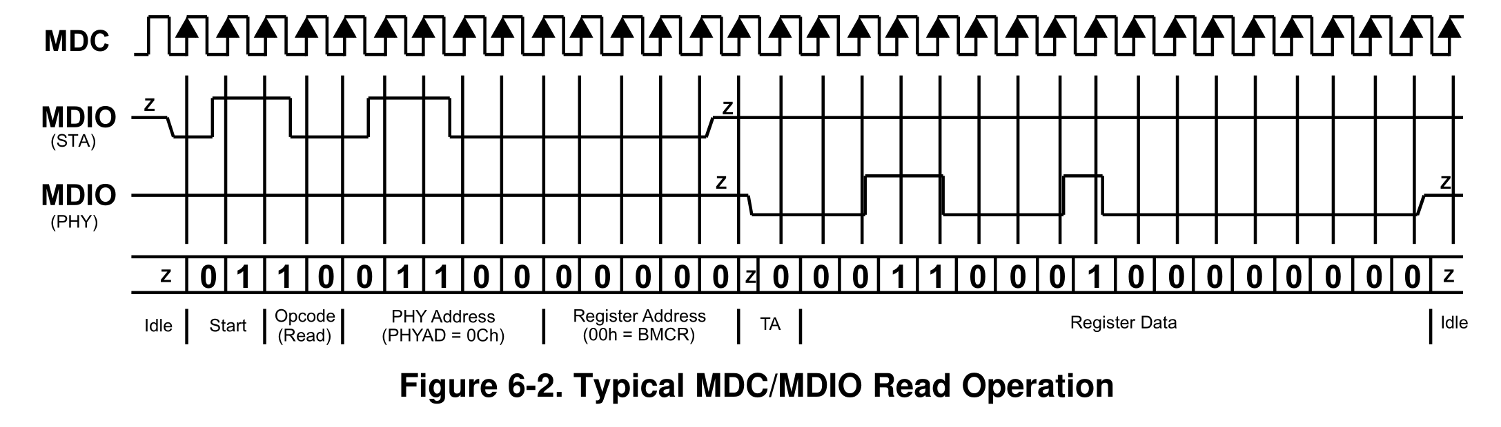
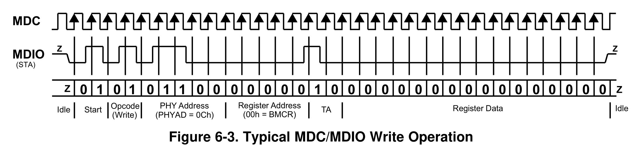
At a high level, data is read/written on the rising edge of the MDC clock and the state machine needs to coordinate when to put the MDIO pin in high-Z to read data transmitted by the PHY. MDIO is much slower than MII and did not require explicit configuration of pin timing constraints. However, the state machine does update the MDIO pin on the falling edge of MDC to ensure timing is respected.
Testing and Validation
In order to test the MDIO master module entirely in simulation, a Bus Functional Model (BFM) was built. The BFM served as a mock ethernet PHY. This allowed for the development and verification of the module’s output timing diagrams to be done entirely in ModelSim. This greatly increased iteration speed as simulation compile times are significantly faster than deploying to hardware. Moreover, the testbench used to verify the design is written using VUNIT and has assertions to show the BFM received the correct data in the correct sequence from the MDIO master module. With GitHub actions, this test runs on every commit providing protection from regressions.
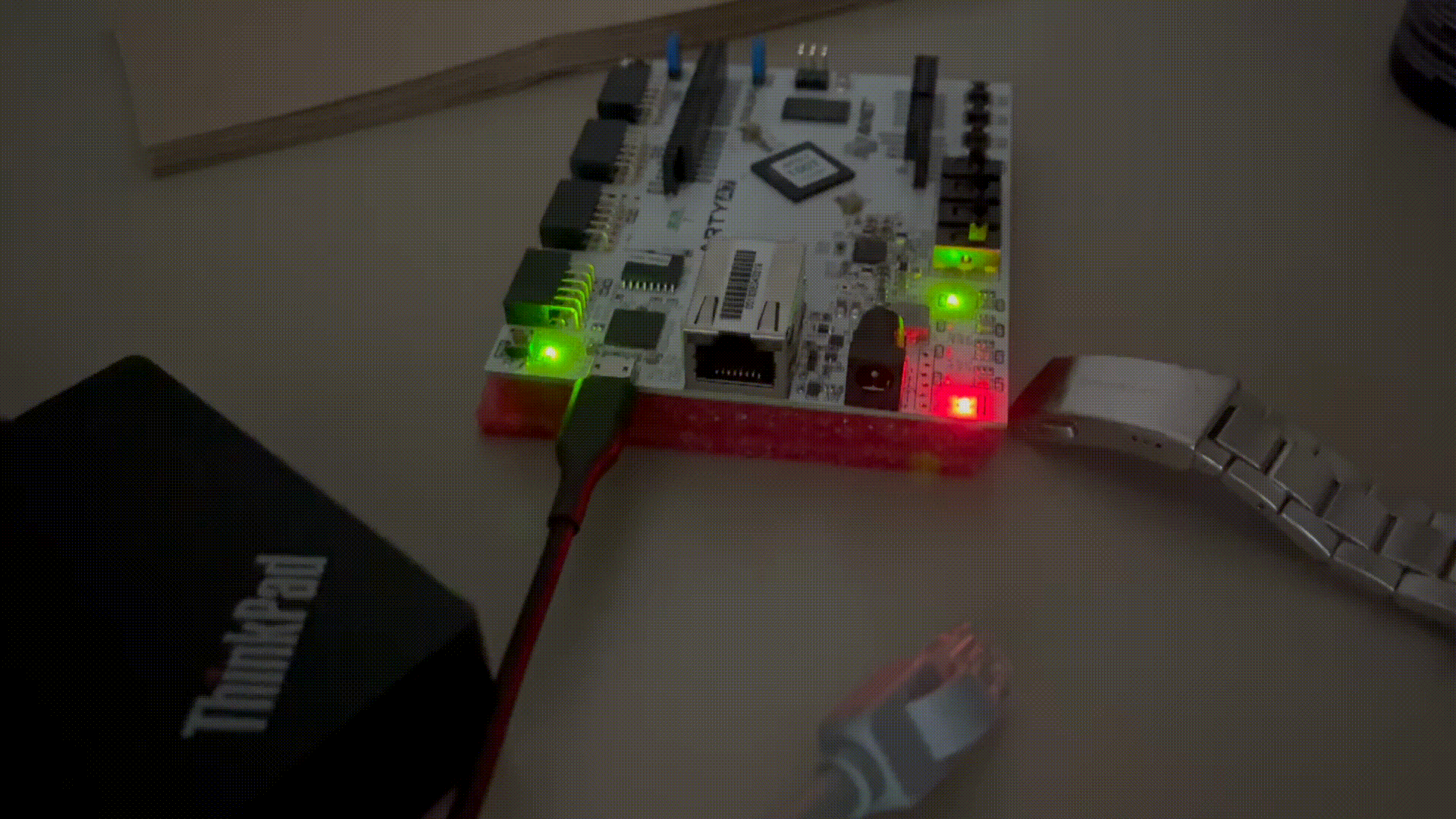
When deploying to hardware, the MDIO module worked as expected on the first try proving the accuracy of the simulation and BFM. As a demo, I wrote this code, which uses the module’s AXI lite interface to write the LED control registers on the ethernet PHY and blink the link LED on the RJ45 connector. The GIF below shows the link LED blinking even though no cable is connected.
Conclusion
Overall, building out the peripherals repository helped me improve my understanding of FPGA development while providing a useful library for future projects. I look forward to sharing additional FPGA projects that build upon these tools!