A Better Arduino: Building a Custom Debugger (Part 2)
Introduction
In part 1 of the “A Better Arduino” series, I designed the simplest possible STM32F7 breakout board. This first iteration PDP board is not nearly as easy to use as an Arduino. The primary problem that users must first properly wire a debugger to the PDP to flash their code. The secondary problem is the lack of serial / USART functionality to do IO with the host machine. The goal of the debugger project is to address these issues by implementing a debugger on a custom circuit board that implements serial communication. Such a circuit could later be embedded into an all in one development solution with the plug and play functionality of Arduino in conjunction with a fully featured debugging suite. I completed the debugger project in order for it to be used by the Queen’s Formula team. The ultimate goal is to lower the barrier to entry of STM32 for new team members so that they can leverage all of its extra capability without any added complexity.
Design
The design of the debugger was quite straight forward as the ST-Link debugger circuit used by STM32 is standardized. The resources I referred to in order to produce the schematic are listed below.
- Nucleo F446RE Development Board Reference Design (built in debugger)
- Design your own ST-Link/V2 Debugger
- Build a mini ST-LINK/V2 programmer/debugger for the STM32
I mainly used the Nucleo reference design as the other two posts listed above did not make use of a UART pass through. All the ST-Link reference designs use an STM32F103C8T6, which is a cortex M3 MCU. This MCU is the standard on both STM32 development boards and standalone debuggers. A screenshot of the ST-Link reference schematic from ST is given below.
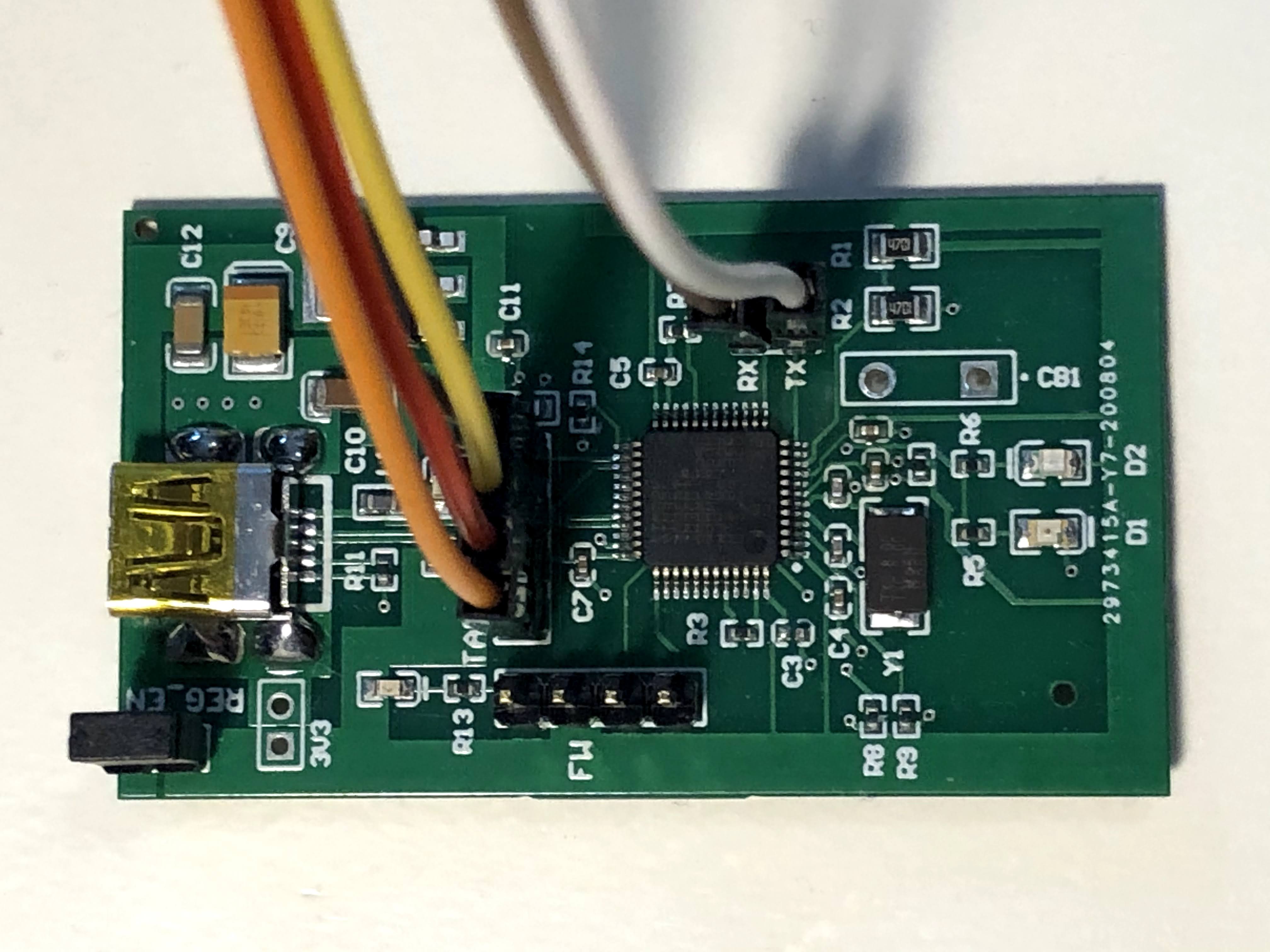
The parts of the schematic that require the most attention is the USB
connection, USART passthrough, Serial Wire Debug (SWD) connection to the target
MCU and SWD connection to the debugger’s MCU, which is used to flash ST-Link
firmware. The USB connection is not fully shown in the above schematic, but only
consists of the D+ and D- differential pair needed for USB 2.0. In the final
debugger design, I added series 22 Ohm resistors and passed the power through a
ferrite bead to reduce noise. However, I have seen working designs that do not
include the resistors or ferrite, but it is best practice to include them in
your USB circuitry. The USB nets are marked as USB_DP and USB_DM, which are
connected to PA12 and PA11 respectively on the MCU. The USART passthrough is
implemented by connecting USART2 on the debugger MCU to a USART on the target
MCU. In the case of the custom debugger board, USART2 is just broken out to a
two-pin header. On the schematic above, the USART nets are marked by STLINK_TX
and STLINK_RX, which are connected to PA2 and PA3 corresponding to USART2 on
the debugger’s MCU. With this connection established, the debugger firmware will
“forward” whatever it receives from the USART on the target MCU to the host
machine. The debug connection to the target is an SWD connection, which consists
of a clock (SWCLK) and data (SWDIO) line. The reference schematic names the pins
in terms of JTAG and includes some extra connections for full JTAG connectivity.
It should also be noted that there are two SWD connections on the debugger’s
MCU. The second connection will be used for programming the debugger’s MCU with
the ST-Link firmware. The target connection is differentiated from the debugger
MCU by leading the target net names with T_ and the debugger ones with STM_.
Since the pins are named using JTAG convention, we need to find what JTAG pins
are equivalent to the two SWD connections. As expected, the SWD and JTAG clock
lines are the same, therefore TCK = SWCLK. Moreover, JTAG data and SWD data are
equivalent, thus, TMS = SWDIO. As a result, T_JTMS is the SWDIO connection
to the target and T_JTCK is the target SWCLK. Similarly, STM_JTMS on the
reference schematic is the SWDIO to the debugger’s MCU and STM_JTCK is the
debugger’s SWCLK connection. Both these SWD connections were copied to the
debugger schematic. Both the target and debugger SWD connections are broken out
on headers labelled with silkscreen. For the net naming, I used an identical
convention to the reference design.
With the debugger functionality implemented in the schematic, the final step was to power the MCU. 100 nF decoupling capacitors are placed on each VDD pin of the debugger’s MCU. The input voltage from the USB connection is 5 V and the MCU logic level is 3.3 V. Thus, I selected an LDO for voltage regulation that JLCPCB stocks in their library so I could send the final board out for assembly. To learn more about JLCPCB’s SMT assembly service, check out my post on using the service here.
Project Viewer
Below is an embedded view of the debugger project which includes the schematic documents, PCB layout and bill of materials. The raw Altium Designer files can be found here. The structure of the debugger Altium project differs from my previous posts as it uses multiple schematic sheets. This is known as a hierarchal schematic design. Each sheet contains a sub-circuit which is tied to other sub-circuits in the parent schematic sheet, which allows for functionality to be divided and organized in smaller schematic documents for larger designs. The sub-circuits are tied together using ports and sheet symbols. A port is similar to a net label, but is used for making connections between schematic sheets instead of normal net labels whose scope is limited to the given sheet. Sheet symbols are used to to take a circuit in another sheet and place it in the current schematic. Ports are then used to connect to the internal nets of the sheet symbol.
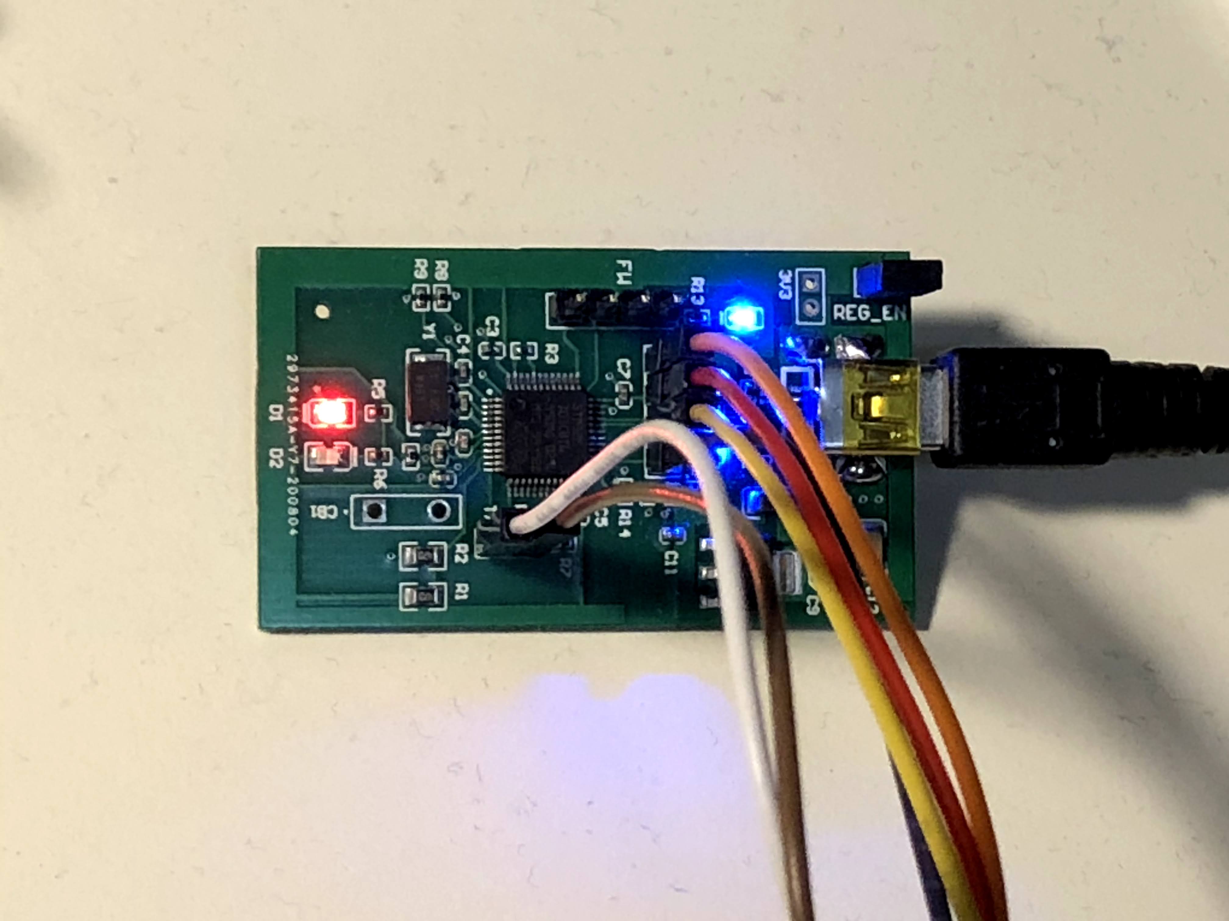
The debugger was ordered with the JLCPCB SMT Assembly service, a photo of the first prototype is given below. You may notice a few small differences between the layout presented in the embedded project compared to the physical board. This is because the board is actually an earlier iteration of the debugger for personal use and testing. The layout presented above includes a few small revisions that I made for the debugger’s wider use by the Queen’s Formula Team. The primary difference lies in the silk screen, which is more descriptive by including a full pinout for each connector on the bottom of the board and Queen’s Formula logo. In addition to aesthetic changes in the silkscreen, there are also some small layout tweaks, with the main change being the regulator enable jumper, which was removed after the LDO circuit was verified to be correct. Another small layout change was switching out the reset jumper for a button.
All of the surface mount components in the figure above were soldered by JLCPCB, with the exception of the USB connector, which was not available from JLCPCB and done by hand.
Software and Board Bring Up
The board testing and bring up can be summarized in the steps listed below.
- Power on Test
- ST-Link Firmware Upload
- Test Connection to Target
- Test USART Passthrough
Power on Test
The power on test went smoothly on the newly delivered debuggers. A USB connector was soldered to each of the 5 units from JLCPCB and then connected to a USB port. The 5 and 3.3 V power LEDs lit up, thereby properly indicating the correctness of the regulator/power circuit. An example of a powered up debugger can be found in the thumbnail for this post.
ST-Link Firmware Upload
The ST-Link firmware is not open sourced by ST. Thus, it can only be obtained by pulling the binary off an existing debugger or from another source that has already completed this process. This blog post has instructions on where to find the firmware. The closed source nature of the software prevents me from linking to the binary directly. The upload of the debugger firmware worked as expected by connecting this ST-Link debugger to the debug header of the debugger’s MCU. After uploading, the debugger board was connected directly to the computer via USB and detected properly by the ST-Link Windows utility provided by ST.
Testing Connection to a Debug Target
I tested the debugger by connecting it to the PDP Board as a test target. The embedded video below shows the debugger successfully connected to the PDP in through ST-Link Utility program while also supplying power to the PDP through its 3.3 V output.
Testing the USART Passthrough
Unfortunately, the initial USART passthrough test with ST-Link firmware did not work. I subsequently discovered that there is a different ST-Link firmware binary needed to support the USART passthrough. Due to the firmware being closed source, my only option was to pull it off a development board that already had the firmware, as I was unable to fnd it online. A comprehensive series of blog posts on capturing the ST-Link with COM port support can be found here. The post mentions a way of getting equivalent functionality without ST-Link through the Black Magic Probe project (Hereby referred to as BMP). The BMP project is open source and supports USART passthrough. Conveniently, the project already had a build profile for turning ST-Link debuggers into BMPs. I followed a tutorial and uploaded the BMP firmware to my debugger board. Unfortunately, only the USART passthrough worked but not debugging and upload. After probing my board, I found that the BMP firmware uses different pin assignments for the SWD pins. Specifically, they use a different pin for clock. Since the project is open source, I modified the pin definitions and recompiled the firmware. The final result is a fully working board with serial and debug support. For those curious about the small change I made to the code, you can see the commit diff on my fork of the BMP repository here.
Conclusion
Overall, the debugger project is a great step towards an easy to use development platform built on top of STM32. Future posts will involve integrating the debugger into STM32 development boards and setting up a software workflow with the black magic probe debugger.