Flex PCB Equalizer
Purpose
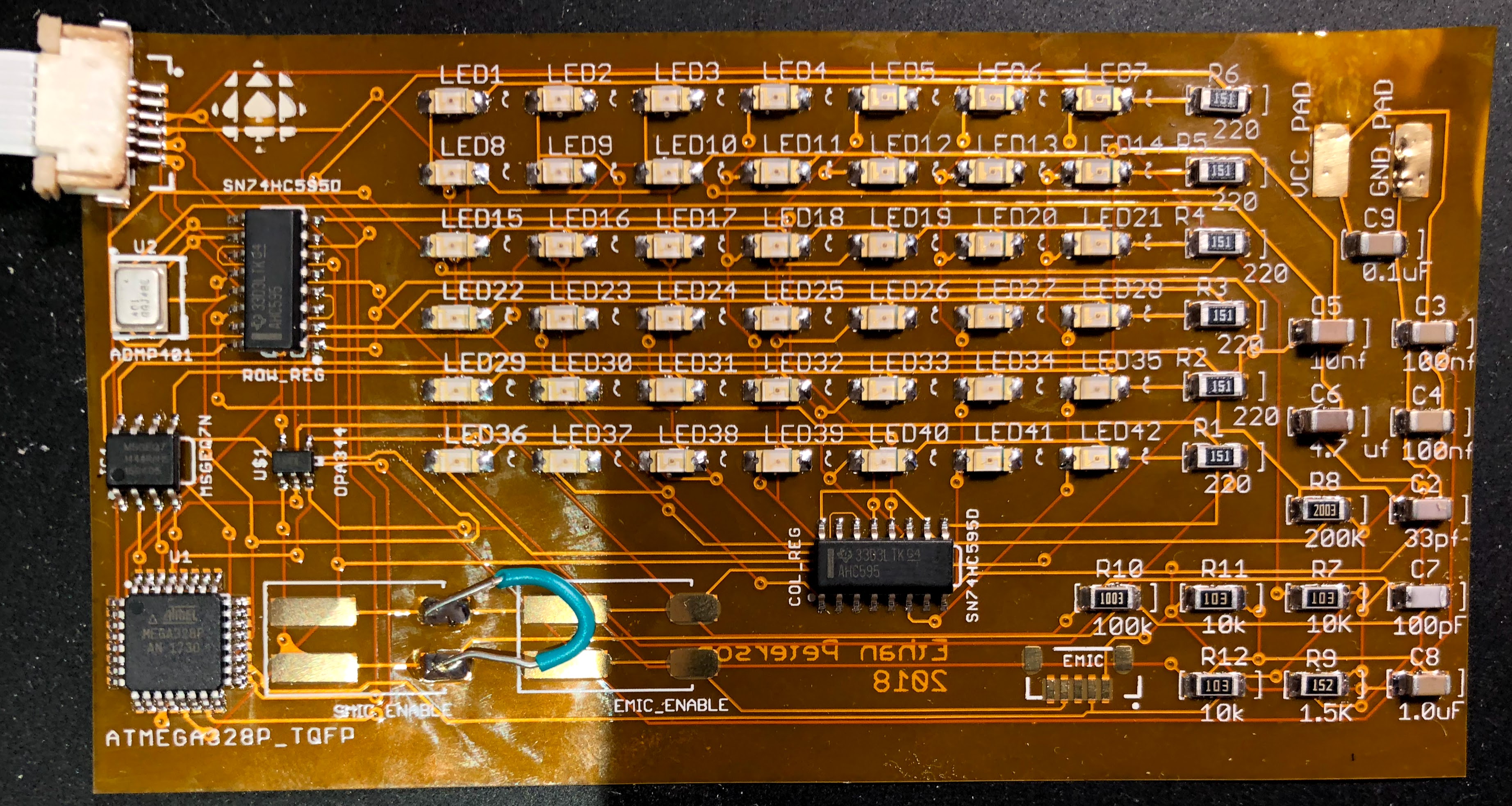
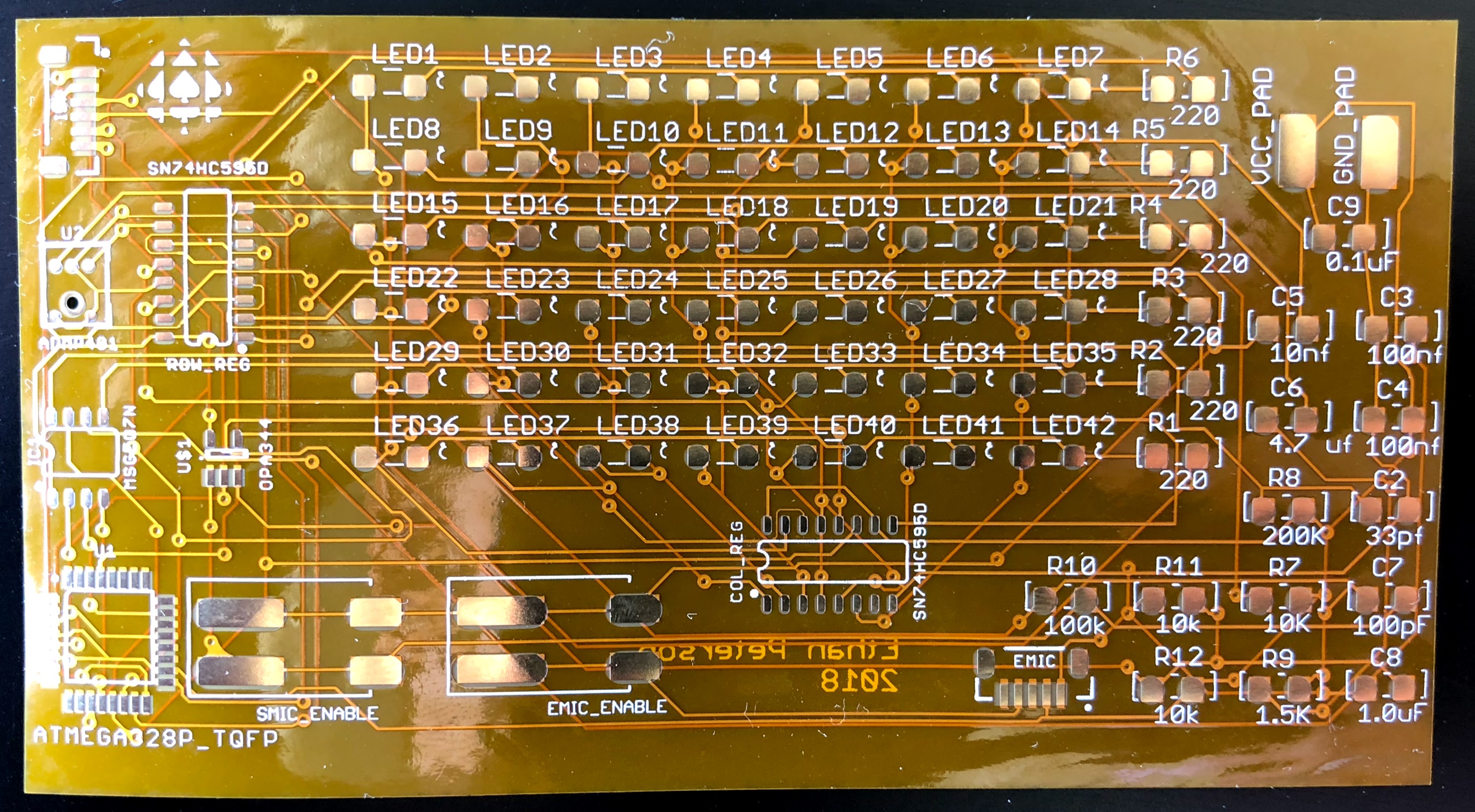
The purpose of the Flex Equalizer Project (referred to in this report as the “FE Project”) is to provide a unique project embedded right into the undersigned’s engineering report, thus developing the critical skills of surface-mount soldering and design on flexible PCBs. The undersigned’s particular flex PCB design is a flexible equalizer building on top of the original GE Project. The PCB is shown below:
| Parts List |
|---|
| 100k Ω Resistor |
| 200k Ω Resistor |
| 1.5k Ω Resistor |
| 3 x 10k Ω Resistors |
| 6 x 220 Ω Resistors |
| MSGEQ7 IC |
| ADMP401 MEMS SMD Microphone |
| OPA344 Amplifier |
| 330 Ω Resistor |
| 470 Ω Resistor |
| 3 x 100 nF Capacitors |
| 33 pF Capacitor |
| 10 nF Capacitor |
| 100 pF Capacitor |
| 4.7 uF Capacitor |
| 2 x 595 SMD Shift Registers |
| ATMega328PB TQFP |
| 42 x 1206 SMD LEDs |
The first skill of PCB design was highly improved upon in the FE Project due to the high complexity of this circuit unifying an LED matrix and equalizer circuitry. The addition of unfamiliar surface mount components that had not been tested in the prototype only made this more challenging.
The second skill acquired in the creation of this project was surface mount soldering. The undersigned had little to no surface mount experience heading into this project, thus making the soldering process difficult but important and rewarding.
The third and most important skill improved upon in this project was assembly programming. A second iteration of the equalizer code was written in AVR assembly, which presented a unique challenge and opportunity to gain a stronger understanding of low-level usage of the ADC (analog to digital converter).
Reference
Sparkfun SMD Microphone Breakout
Procedure
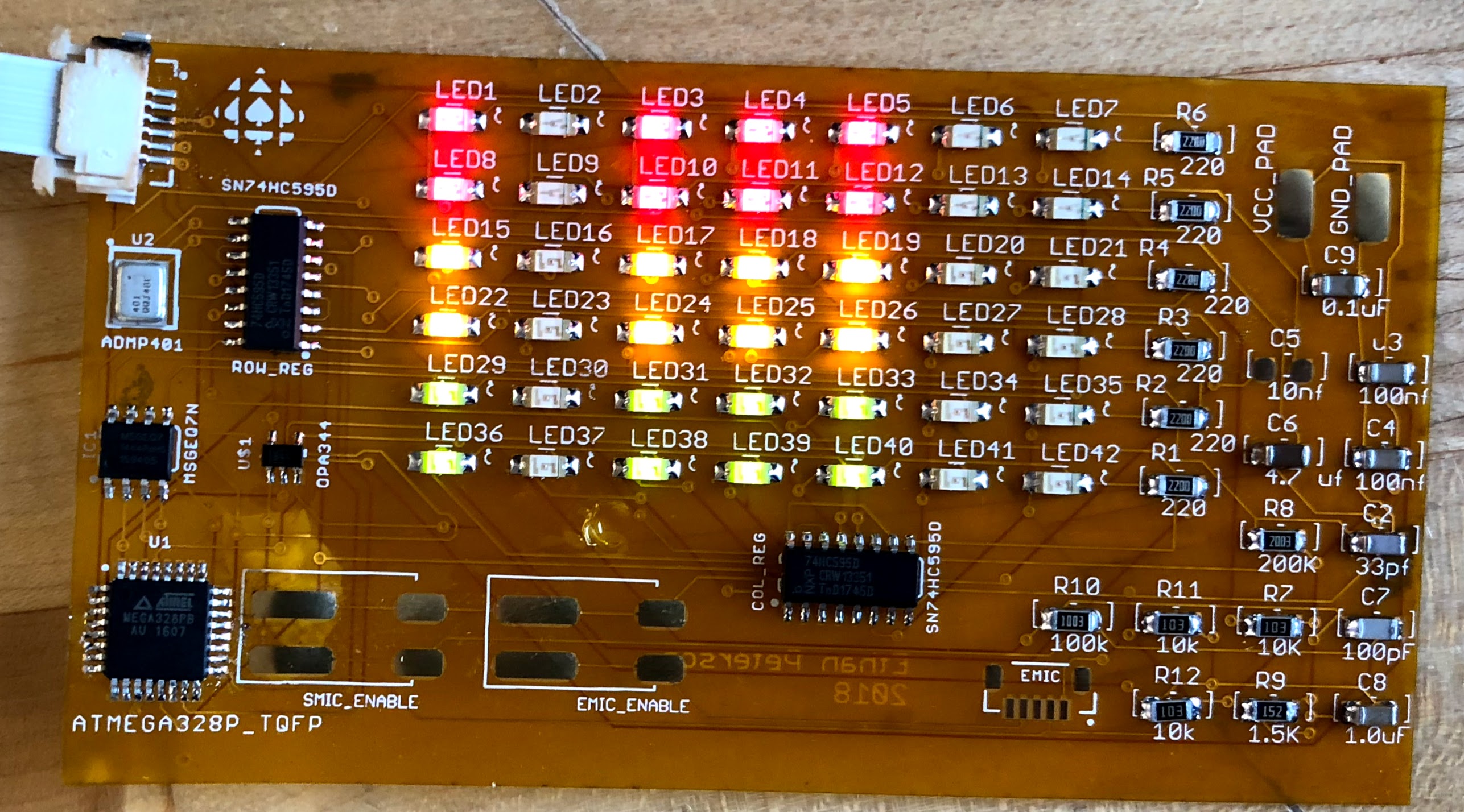
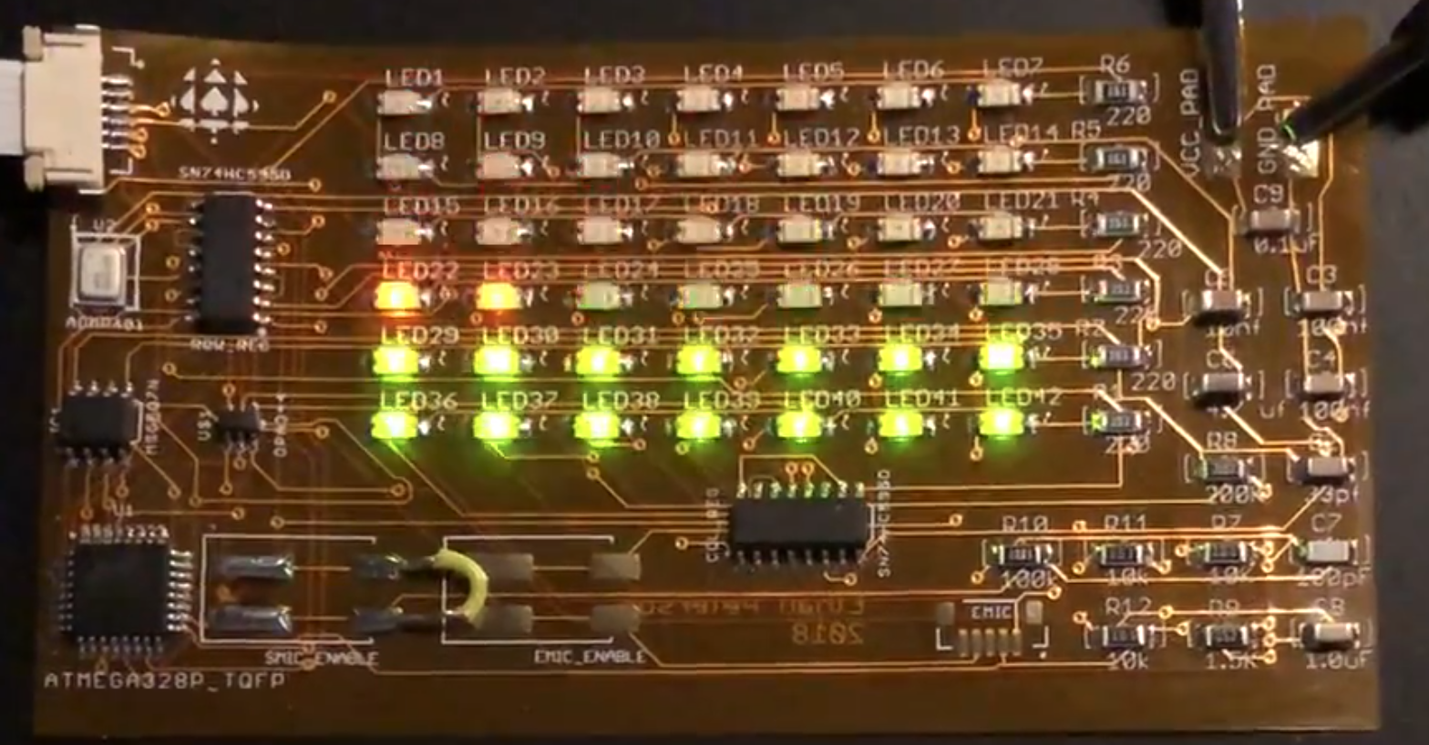
The FE Project improves upon the original GE Project developed in the TEI3M course. The FE used in the project is also a graphic equalizer, however, it is mounted on a flexible PCB using fully surface mount components so it can be laminated into a page in the undersigned’s engineering report. The second key difference between the FE and its through-hole predecessor is the usage of a 7x6 LED Matrix to display audio levels as opposed I2C based bar graphs. The use of a multi-plexed LED Matrix with standard shift registers also eliminates the need for libraries in order to write code for the FE, thus allowing the code to be re-written as mid-level AVR C or AVR Assembly.
The development of the FE Project is comprised of four important steps, consisting of prototyping, PCB design, soldering and programming.
The first of three difficult steps to complete the FE Project was prototyping. Although the undersigned completed an equalizer project on two occasions and completed similar circuits on several occasions, there were new obstacles to overcome in completing a properly functioning surface mount version. The first challenge was outputting to an LED matrix, which was summarily bypassed thanks to an LED matrix Arduino shield that the undersigned had previously developed, thus avoiding a copious amount of extra wiring. The second difficulty related to power delivery. Since the FE Project would ultimately be powered by a flexible solar panel that only provides 3.7 V as opposed to 5, it had to be confirmed that the circuit did not require the extra voltage or current. Fortunately, at the cost of LED brightness, the prototype still operated by drawing a small enough current that the solar panel was adequate under very bright sunlight. The final and most difficult obstacle was finding specialized surface mount components to replace the corresponding through-hole counterparts. The MSGEQ7 frequency analyzer chip was difficult to find in a SMD package along with a compatible SMD microphone. Microphones tested in the prototyping process failed to provide proper amplification, thus leading to an unresponsive equalizer. Eventually, a Sparkfun breakout board was found that employed an SMD microphone and used a separate amplifier chip for a strong signal. The undersigned was unable to obtain this board during the prototyping process so a through-hole microphone with amplification was used to emulate the surface components that had not yet arrived. As the circuit for the Sparkfun breakout board was posted online, it could later be integrated into the undersigned’s flex PCB. Programming the prototype was a straightforward process thanks to the use of Arduino C and previous experience programming these types of devices.
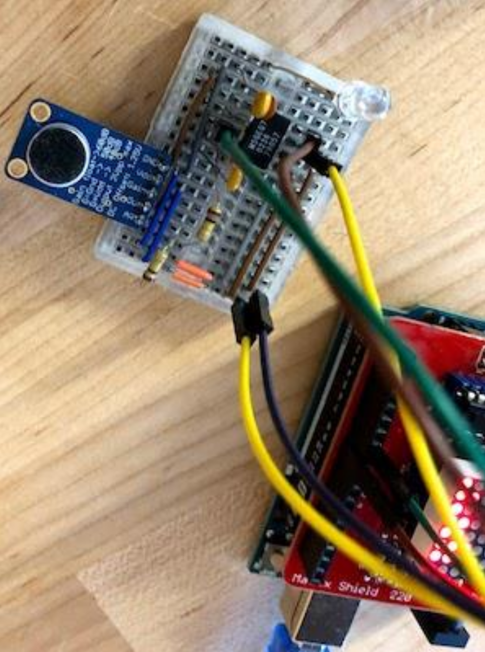
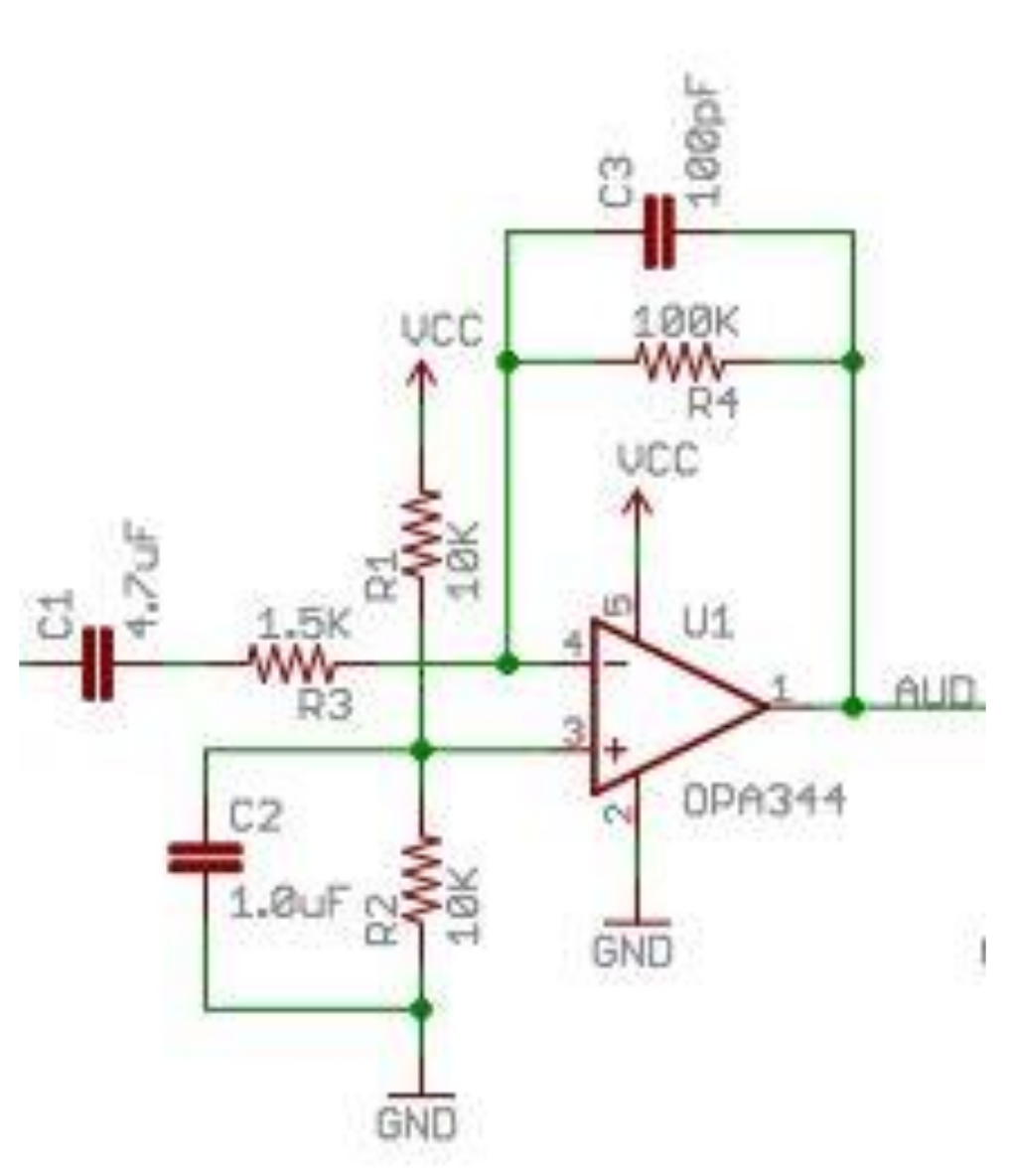
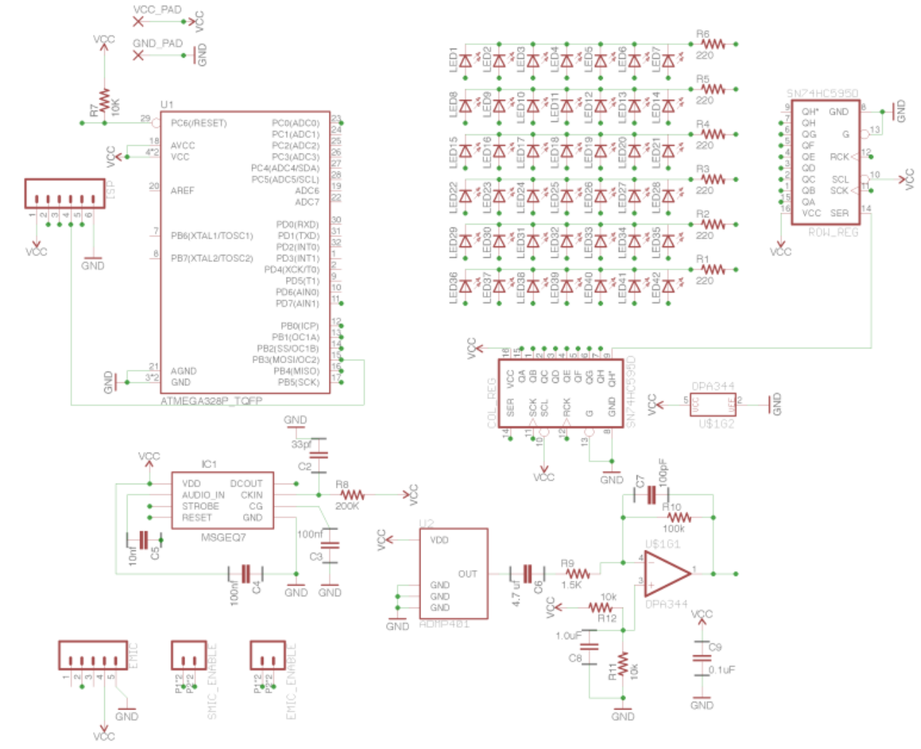
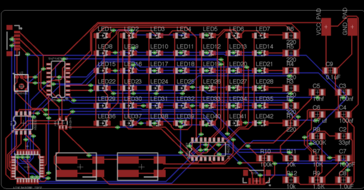
The second step was to design the FE in EAGLE, starting with a circuit diagram. First, a 7 x 6 LED matrix was created using 1206 SMD LEDs. The matrix was then connected to two SMD 595 shift registers in a multi-plexed configuration. The two shift registers were daisy-chained together, thus allowing them to occupy only 3 pins on the ATmega328PB Microcontroller. Secondly, the equalizer component of the circuit had to be created. The MSGEQ7 was added to the circuit and wired in an identical manner to previous equalizers. The FE presented a unique problem in getting the microphone output into the MSGEQ7. The SMD requirement for the flex page prevented the use of a through-hole microphone breakout board employed in previous equalizers. As a result, extra circuitry needed to be added to amplify and support the ADMP401 SMD microphone. The extra circuitry is pictured below.
The third step was completion of all soldering work upon delivery of the flex PCB. The PCB has a dense and very small form factor, with many components placed closely together. Placing the solder paste on each pad individually proved to require too much precision to do completely by hand. As a result, the task was completed with the use of a stencil. The stencil for the board is a custom cut aluminum sheet which has a hole for each pad on the PCB. The flex PCB is prepared for soldering by taping the PCB to the back of the stencil and aligning each pad with the corresponding hole on the stencil. Once the board is mounted to the stencil, solder paste is placed on top of the stencil and spread across it using a squeegee. The paste is spread until it has sunk through the holes on the stencil and onto the pads on the PCB. With solder paste placed on the PCB, the components could then be mounted to be soldered via hot air. Each SMD component was placed on its corresponding pads using tweezers. Once all the components were placed on the board, the hot air gun was used to melt solder paste and solder the components. All the components fell into place without any bridging of the pads, with the exception of the ATmega328PB TQFP microcontroller. A few pads were bridged on the microcontroller, thus causing a short circuit which was corrected by using solder wick to un- bridge the pads. However, it should be noted that the exposure of the PCB to some heat during this repair process caused some warping in the area where the microcontroller is located, but no traces were destroyed.
The final and most difficult step of the project was programming and debugging
the FE. The FE worked well initially using Arduino C code. As the undersigned
had written equalizer code on multiple occasions, it was decided to take the
code to lower level assembly. The assembly was nearly complete when the ability
to program the ATmega328PB on the PCB was lost. The issue arose when the flex
cable was removed from the ISP connector of the original board and connected to
the second FE board that had just cooked in the reflow oven. Unfortunately, when
the flex cable was reconnected to the original board, code would no longer flash
on the Arduino IDE and no result was shown after flashing the code successfully
in Atmel Studio. After many hours of troubleshooting, it was discovered that an
issue in the code prevented the PCB from showing any signs of functionality.
This fix only exposed many more underlying problems with ISP flex ports on the
board. The port and flex cable had very weak electronic connections, making it
difficult to program the on board microcontroller. However, the first FE board
to be soldered was beyond repair and no longer functioning. Although the second
PCB was programmable, the connections were too weak to exit debugWire mode since
the ICE was unable to read the device signature properly and disable the DW
fuse. The microcontroller being locked in this mode proved to be difficult as it
reduced the chip’s clock speed and removed the option of using ISP mode to
program the chip with high level code from the Arduino IDE. Fortunately, the
assembly code worked, but the reduced clock speed remained an issue. POV
(persistence of vision) was restored to the matrix by reducing the prescaler to
8 from 1024 on Timer0, which schedules ADC readings. The prescaler change made
everything appear to run faster but the issue was fully fixed when the F_CPU
value was redefined at the top of the code forcing a clock speed of 8 Mhz. With
one board up and running, it was time to repair the third board so two working
boards could be submitted to the course instructor. This board also suffered
from a weak ISP connection. To address the issue, a fresh ISP adapter was
soldered and a new flex cable was used so that the connection could be as strong
as possible. Unfortunately, the third board still did not program. Each solder
link was examined with a magnifying glass. This lead to the discovery that the
solder paste on the reset pin of the ATmega328P had not fully melted, thus
making for a weak connection to a pin integral for programming the
microcontroller. The hot air rework station was used to touch up this link,
thereby allowing code to be successfully flashed onto the chip. The assembly
code for the project was difficult to develop but much easier to debug once
hardware issues with the PCB had been fixed. The assembly code consisted of two
interrupts, a timer interrupt to schedule new ADC readings and an interrupt when
the ADC completed a reading. Each time the ADC completed a reading, the code in
the ADC_Complete label would run. The code in the label would copy the reading
to a general purpose register and map the reading to a value from 0 – 5. Once
the reading is collected, another label called showBand is run using the rcall
instruction. showBand takes the reading and displays it in the appropriate
column of the LED Matrix based on the frequency which was read from the MSGEQ7.
The label knows what column to enable based off of the currentCol register,
which shifts a single bit left each time a new reading is collected from the
MSGEQ7 so that the next column over is enabled. The mapped reading value is then
used to turn on the appropriate number of LEDs within the corresponding column
of the LED Matrix.
Media
Code
The source code can also be found on the undersigned’s GitHub repository.
#include "prescalers.h"
#define F_CPU 8000000UL ; Define CPU frequency
.cseg
  .org 0x0000
    rjmp reset
  .org 0x0020
    rjmp TIM0_OVF
  .org 0x002A
     rjmp ADC_Complete

.org 0x0040 ; start past interrupt vector table

.equ data = 3 ; PORTB
.equ latch = 2
.equ clk = 1

.equ strobe = 0 ; PORTB
.equ resetPin = 7 ; PORTD

.def cols = r16
.def rows = r17
.def reading = r18
.def working = r19
.def currentBand = r25
.def currentCol = r24

reset:
  cli ; disable interrupts while they are being set up
  ldi currentCol, 1
  rcall initPins
  rcall ADCInit
  rcall T0Init
  rcall initMSG
  sei ; enable interrupts after they have been configured
  rjmp wait ; jump into the main code

; Replace with your application code
; MSBFIRST Shiftout function handling both row and column registers (16 pins)
.MACRO shiftOut
  cbi PORTB, latch

  ; handle shifting data
  cbi PORTB, clk
  cbi PORTB, data
  sbrc @0, 7 ; skip if bit in register passed to macro is cleared
  sbi PORTB, data
  sbi PORTB, clk

  cbi PORTB, clk
  cbi PORTB, data
  sbrc @0, 6 ; skip if bit in register passed to macro is cleared
  sbi PORTB, data
  sbi PORTB, clk

  cbi PORTB, clk
  cbi PORTB, data
  sbrc @0, 5 ; skip if bit in register passed to macro is cleared
  sbi PORTB, data
  sbi PORTB, clk

  cbi PORTB, clk
  cbi PORTB, data
  sbrc @0, 4 ; skip if bit in register passed to macro is cleared
  sbi PORTB, data
  sbi PORTB, clk

  cbi PORTB, clk
  cbi PORTB, data
  sbrc @0, 3 ; skip if bit in register passed to macro is cleared
  sbi PORTB, data
  sbi PORTB, clk

  cbi PORTB, clk
  cbi PORTB, data
  sbrc @0, 2 ; skip if bit in register passed to macro is cleared
  sbi PORTB, data
  sbi PORTB, clk

  cbi PORTB, clk
  cbi PORTB, data
  sbrc @0, 1 ; skip if bit in register passed to macro is cleared
  sbi PORTB, data
  sbi PORTB, clk

  cbi PORTB, clk
  cbi PORTB, data
  sbrc @0, 0 ; skip if bit in register passed to macro is cleared
  sbi PORTB, data
  sbi PORTB, clk

  cbi PORTB, clk
  cbi PORTB, data
  sbrc @1, 7 ; skip if bit in register passed to macro is cleared
  sbi PORTB, data
  sbi PORTB, clk

  cbi PORTB, clk
  cbi PORTB, data
  sbrc @1, 6 ; skip if bit in register passed to macro is cleared
  sbi PORTB, data
  sbi PORTB, clk

  cbi PORTB, clk
  cbi PORTB, data
  sbrc @1, 5 ; skip if bit in register passed to macro is cleared
  sbi PORTB, data
  sbi PORTB, clk

  cbi PORTB, clk
  cbi PORTB, data
  sbrc @1, 4 ; skip if bit in register passed to macro is cleared
  sbi PORTB, data
  sbi PORTB, clk

  cbi PORTB, clk
  cbi PORTB, data
  sbrc @1, 3 ; skip if bit in register passed to macro is cleared
  sbi PORTB, data
  sbi PORTB, clk

  cbi PORTB, clk
  cbi PORTB, data
  sbrc @1, 2 ; skip if bit in register passed to macro is cleared
  sbi PORTB, data
  sbi PORTB, clk

  cbi PORTB, clk
  cbi PORTB, data
  sbrc @1, 1 ; skip if bit in register passed to macro is cleared
  sbi PORTB, data
  sbi PORTB, clk

  cbi PORTB, clk
  cbi PORTB, data
  sbrc @1, 0 ; skip if bit in register passed to macro is cleared
  sbi PORTB, data
  sbi PORTB, clk

  sbi PORTB, latch

.ENDMACRO

wait: ; full equalizer code takes place within interrupt service routines
  rjmp wait

initPins: ; set I/O pins being used to output
  sbi DDRB, data
  sbi DDRB, latch
  sbi DDRB, clk
  sbi DDRB, strobe
  sbi DDRD, resetPin
ret

; takes mapped MSGEQ7 reading and places it in the right column of LED matrix
showBand:
  clr rows

  ; test the reading value and branch to a label
  cpi reading, 5
  breq rows_5

  cpi reading, 4
  breq rows_4

  cpi reading, 3
  breq rows_3

  cpi reading, 2
  breq rows_2

  cpi reading, 1
  breq rows_1

  cpi reading, 0
  breq rows_0

  ser rows
  rjmp end

  rows_5:
    sbr rows, 1 << 5
    sbr rows, 1 << 4
    sbr rows, 1 << 3
    sbr rows, 1 << 2
    sbr rows, 1 << 1
    sbr rows, 1 << 0
    rjmp end


  rows_4:
    sbr rows, 1 << 4
    sbr rows, 1 << 3
    sbr rows, 1 << 2
    sbr rows, 1 << 1
    sbr rows, 1 << 0
    rjmp end

  rows_3:
    sbr rows, 1 << 3
    sbr rows, 1 << 2
    sbr rows, 1 << 1
    sbr rows, 1 << 0
    rjmp end

  rows_2:
    sbr rows, 1 << 2
    sbr rows, 1 << 1
    sbr rows, 1 << 0
    rjmp end

  rows_1:
    sbr rows, 1 << 1
    sbr rows, 1 << 0
    rjmp end

  rows_0:
    sbr rows, 1 << 0
    rjmp end

  end:
    com rows
    shiftOut rows, currentCol
    ret

ADCInit:
  ser r16 ; set all bits in r16
  ldi r16, (1 << REFS0) | (1 << ADLAR)
  sts ADMUX, r16
  ; Enable, start dummy conversion, enable timer as trigger, prescaler
  ldi r16, (1 << ADEN) | (1 << ADSC) | (1 << ADATE) | (1 << ADIE) | (1 << ADPS2) | (1 << ADPS1) | (1 << ADPS0)
  sts ADCSRA, r16
  ldi r16, 1 << ADTS2
  sts ADCSRB, r16

dummy:
  lds r16, ADCSRA
  andi r16, 1 << ADIF
  breq dummy
  ret

T0Init: ; initialize T0 interrupt to schedule ADC conversions
  clr r16
  out TCCR0A, r16 ; normal mode OC0A/B disconnected
  ldi r16, T0ps8 ;
  out TCCR0B, r16
  ldi r16, 1 << TOIE0 ; Timer interrupt enable
  sts TIMSK0, r16 ; output to mask register to
  ret

TIM0_OVF:
  cbi PORTB, strobe ; make strobe low to grab a frequency band
  rcall delay ; let MSG output settle
  lds r16, ADCSRA ; start an ADC conversion
  sbr r16, 1 << ADSC ; set the required bit
  sts ADCSRA, r16
  reti

ADC_Complete: ; ISR for when a Analog to Digital Conversion completes
  lds reading, ADCH ; grab ADC reading and place in gp reg
  ; map reading value to a value from 0 - 5
  ldi r20, 6
  mul r20, reading
  mov reading, r1 ; load mapped value back into reading register
  rcall showBand
  sbi PORTB, strobe ; pulse strobe pin to grab new frequency band
  inc currentBand
  lsl currentCol ; shift the column bit left to move to the next column
  cpi currentBand, 7
  breq clear
  reti

clear: ; reset MSG after reading all 7 frequency bands
  sbi PORTD, resetPin
  cbi PORTD, resetPin
  ldi currentCol, 1
  clr currentBand
  reti

initMSG: ; prep MSGEQ7 to have to give audio readings in the ADC ISR
  cbi PORTD, resetPin
  sbi PORTB, strobe
  ret

delay: ; 22 uS delay for reading from the MSGEQ7
  ldi r21, 117
  L1: dec r21
  brne L1
  nop
  ret
Conclusion
Overall, the FE Project qualifies as one of the most sophisticated and challenging projects the undersigned has completed in the ACES Program. As a result of the FE Project, an absolutely stronger knowledge of surface mount soldering and assembly programming was developed. With respect to soldering, the undersigned acquired skills in the use of a hot air rework station as well as a reflow oven. With respect to assembly programming, the undersigned acquired skills specifically relating to the use of interrupts and hardware peripherals on microcontrollers, such as the analog to digital converter. More importantly, however, it should be noted that this project has created in the undersigned an unparalleled sense of pride and achievement with regard to one of the final projects as an ACES student.