Assembly Binary Game
Purpose
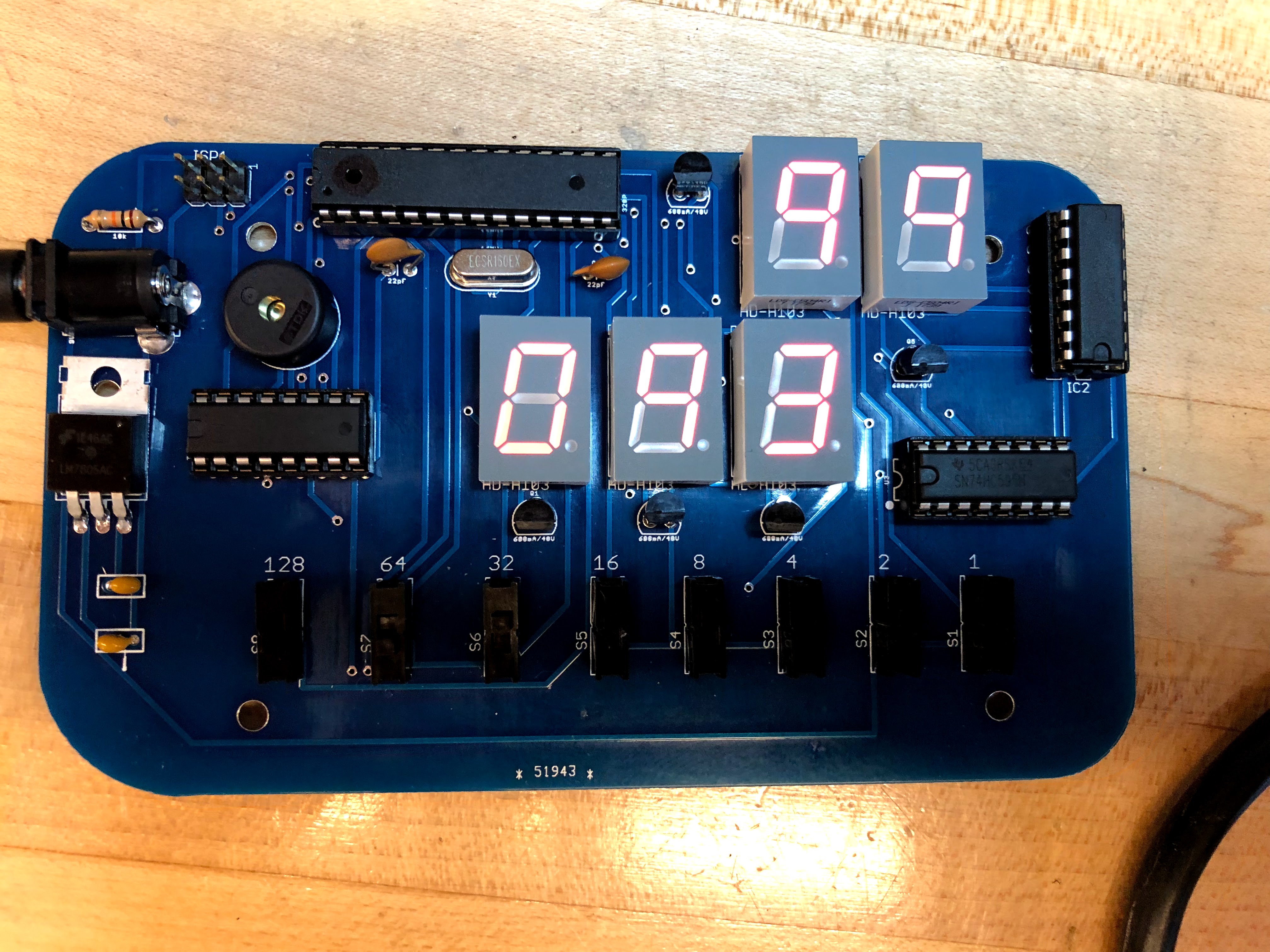
The purpose of the Assembly Binary Game Project (referred to in this report as the “ABG Project”) is to provide a hardware substitute for the now defunct online Cisco Binary Game. The binary challenge was a competition amongst junior ACES where a tournament is held to see who can achieve the highest score in a fixed amount of time. The ABG Project aims to allow students to hold this competition using physical hardware consoles instead of websites like the Cisco Binary Game, which ultimately ended up being placed behind a paywall. The custom PCB allows for many ABG consoles to be created for a potential class set for future ACES students to continue the binary challenge tradition.
| Parts List |
|---|
| 10k Ω Resistor |
| 5 x 3904 BJTs |
| 16 Mhz Crystal Oscillator |
| ATMega328P |
| 2 x 22 pF Capacitors |
| 8 x Switches |
| 5 x 7-Segment Displays |
| 595 Shift Register |
| 2 x 4511 7-Segment Driver |
| 2 x 100 nF Capacitors |
| DC Jack |
| LM7805 Voltage Regulator |
The ABG Project allowed the undersigned to improve both assembly language skills and PCB design skills. As the entire project’s code is written in assembly, the ABG Project serves as a good introduction to writing complex and fully featured programs in assembly language. The PCB was also found to be one of the most complex through hole boards that the undersigned has designed to date, due in part to the large number of components as well as unique and unfamiliar components that were used by the undersigned on the PCB, such as transistors.
Reference
Random Number Generator Example 1
Random Number Generator Example 2
Random Number Generator Example 3
Procedure
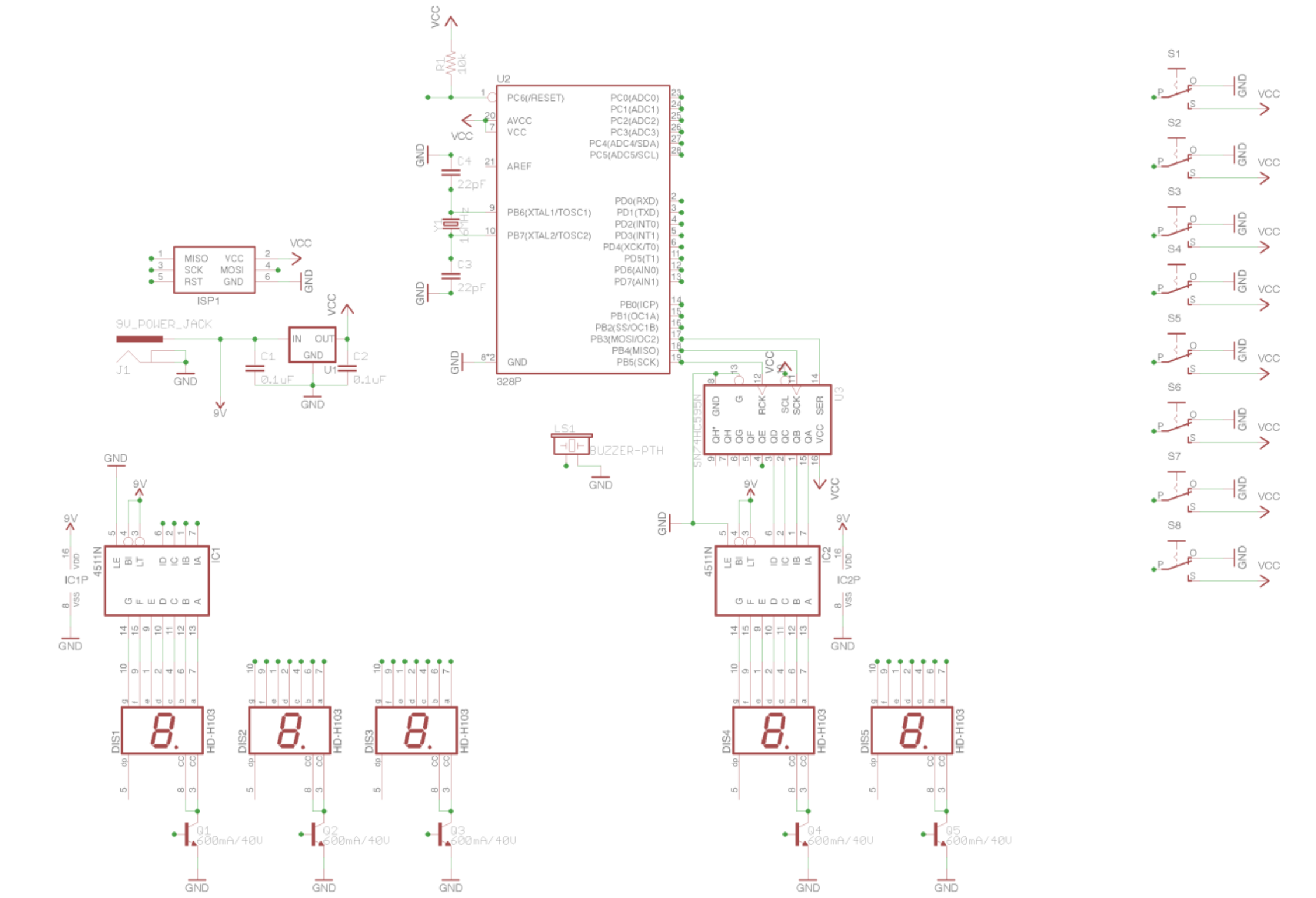
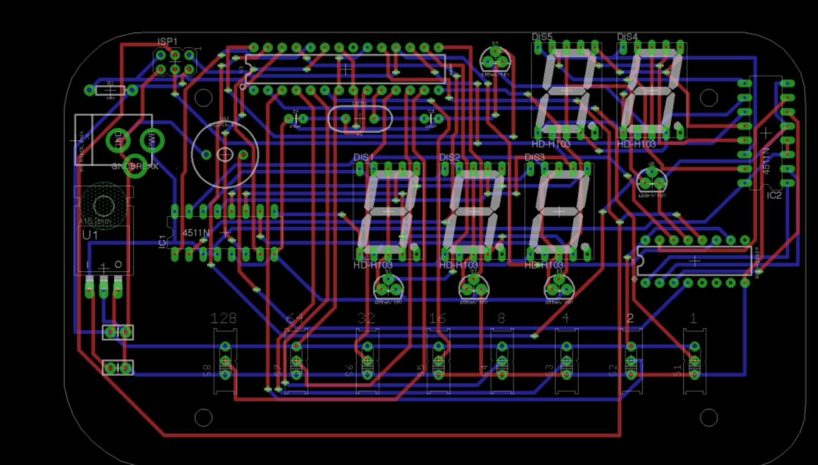
The ABG Project consists of 8 switches for binary number input, seven segment displays for score and the 8-bit number to create in binary using the input switches. The displays are driven by two 4511 7-Segment display driver ICs and a 595 shift register, since many of the ATmega328P’s digital pins are already tied to other components such as the input switches.
The construction of the ABG Project is comprised of 3 steps; prototyping, PCB design and programming.
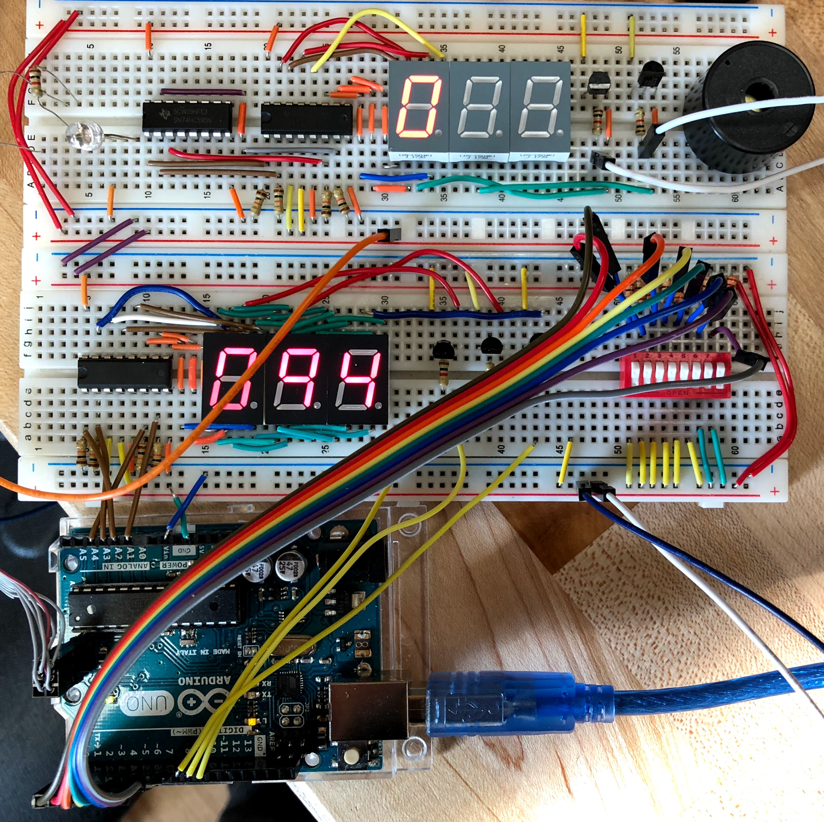
The first and most straightforward step of the ABG Project is the breadboard prototype. First, 3 common-cathode 7 segment displays were connected to the outputs of a single 4511 chip. The cathodes of each display are each wired to one NPN3904 transistor. The base pins of each transistor are connected to PORTB of the Arduino so that a particular display can be selected in code by blocking the path to ground for the other two by leaving their transistor base pins low. The use of transistors allows all 3 displays to be controlled by a single 4511 using POV by switching through the displays showing one digit at a time so quickly that it appears as one number. The input pins of the 4511 are sequentially connected to PORTC. This configuration makes displaying a digit as simple as outputting a value to PORTC. An additional two 7-Segment displays are used to display the player’s score. These two displays are connected to the outputs of another 4511 chip and their cathodes are connected to transistors in the same configuration as the other 3 displays. The only difference in the setup of the score displays is that the inputs of the 4511 are not directly connected to the Arduino, due to a shortage of I/O pins. Instead, the inputs of the 4511 are connected to the first 4 outputs of a 595 shift register, which feeds the lower nibble of the byte shifted out directly to the 4511. The two transistors for selection of a score display are still operated directly by the Arduino connected to PORTC. The final addition to the prototype circuit is an 8-bit DIP switch, which was connected to PORTD of the Arduino sequentially so that the byte inputted by the user could be read with a simple call to the in command.
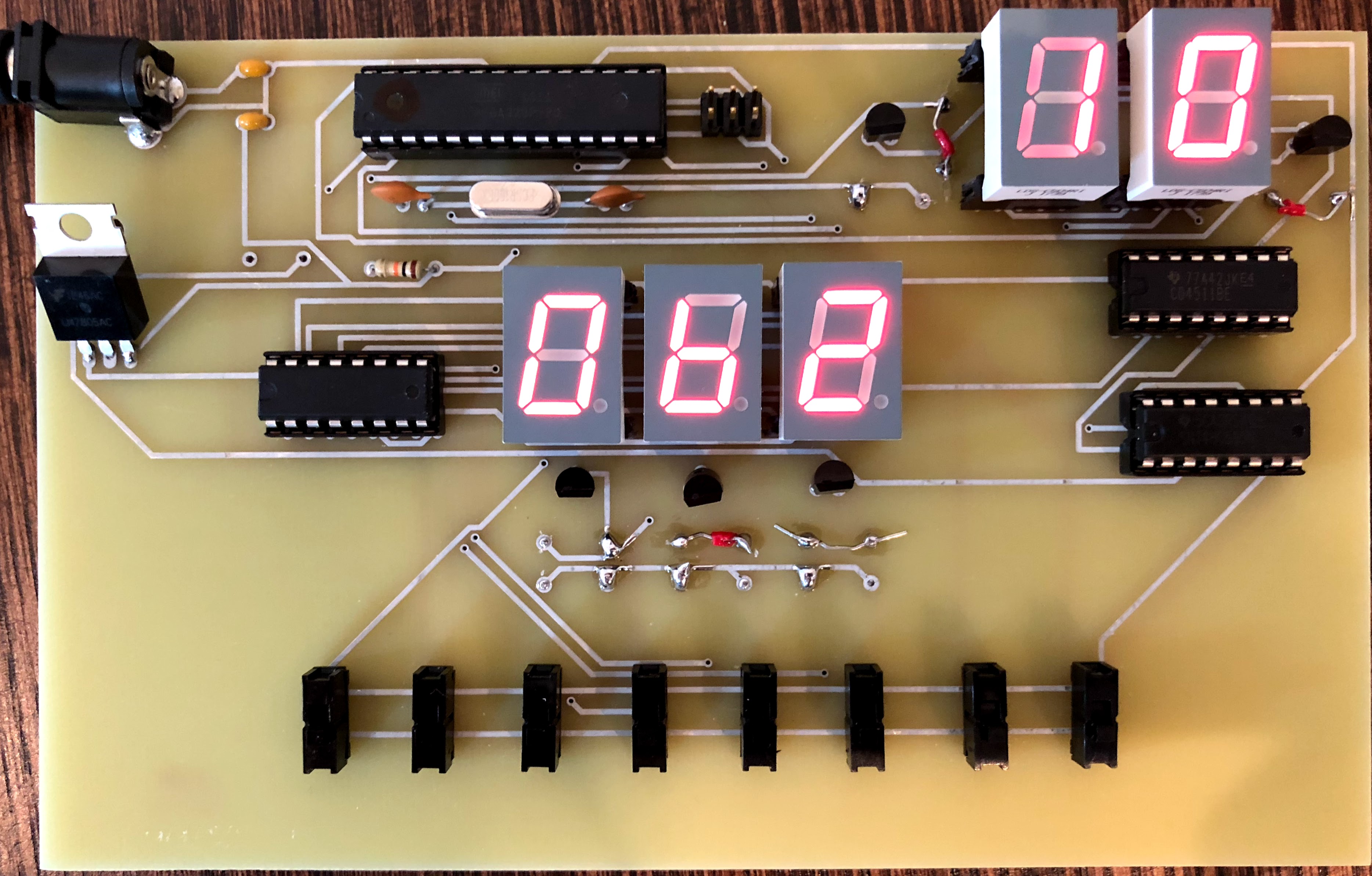
The second step in the construction of the ABG Project is PCB design. The key differences between the prototype circuit and the final EAGLE schematic is the addition of a 5V voltage regulator so the board can receive power from a 9V battery. The Arduino is also replaced with an off board ATmega328P and the accompanying circuitry, such as an ISP header. Notwithstanding the few modifications to the original prototype circuit, the PCB did not fully function when it arrived. The code was seemingly running properly on the board but the displays appeared very dim. This issue was initially attributed to the small trace width of 8 mil being unable to carry enough current to support the 7-Segment displays. As a result, an identical board with larger traces was ordered but the same issue was encountered. Upon further inspection, it was discovered that the dimness resulted from the 1k Ω resistors connected to the base pins of each transistor and the 470 Ω resistors connected to the cathode of each display. Since the PCB had exposed traces, all the resistors were removed and replaced with extra wire connecting the two traces, which lead to the displays running at their normal brightness. A third iteration of the board was immediately ordered to settle the issue completely, however, it did not arrive in time for the creation of this report.
The final and most difficult step of the ABG Project is writing the code for the binary game in AVR assembly. The assembly code is structured in a similar way to an Arduino program with a setup label which initializes all the I/O pins and interrupts, and a loop label where the bulk of the game code runs. The code utilizes two timer interrupts and an ADC interrupt. An interrupt on TIMER2 is configured to run at a frequency of 63 Hz constantly polling for the correct switch combination matching the number being displayed. This interrupt service routine (ISR) also assists in the POV for the displays by running the double dabble algorithm on the new random value, breaking it into its individual digits to be presented via POV in the loop label. The comparison between switch input and the number on display is done using the in command to load the value of the PIND register into general purpose register and compare to the number shown on the displays using the cp command. The breq command is used to branch to a new label called isEqual if the comparison returned true, which increments the score value and loads a new random number to be shown. The random numbers come from random number generator code found on the website “AVR Freaks”, which has been modified to use a random seed from an ADC reading. The use of the ADC requires two interrupts. A timer interrupt from TIMER0 is used to schedule new ADC readings and another ADC ISR runs when that reading is completed. The ISR is called ADC_Complete, which runs when there is a new reading. The new reading is copied into a general purpose register defined as newValue, which is fed as a seed to the random number generator.
Media
Unfortunately, the demo video only includes the first iteration PCB prototype. The blue prototype had not yet arrived when the video was shot.
The full EAGLE project files and source code can be found on the unsersigned’s GitHub.
Code
.cseg
#include "prescalers.h"
.org 0x0000
  rjmp reset

.equ size = 15

.org 0x000E
rjmp TIM2_COMPA

.org 0x002A
rjmp ADC_Complete

.org 0x0020
rjmp TIM0_OVF
.org 0x100

reset:
  clr r22
  ldi r16, low(RAMEND)
  out spl, r16
  ldi r16, high(RAMEND)
  out sph,r16
  movw z,x

.def original = r16 ; value to be pushed through double dabble algorithm
.def onesTens = r17 ; register holding ones and tens output nibbles from double dabble
.def hundreds = r22 ; hundreds output from double dabble
.def working = r24 ; register used to work with data that needs to be preserved
.def addReg = r20 ; holds a value of 3 to be added to other registers in the double dabble process
.def times = r25 ; register holding the number of bit shifts the double dabble algorithm must do before being complete
.def input = r21 ; raw graycode input from rotary encoder
.def newValue = r23 ; where newly generated random numbers will be stored
.def score = r15
.def copy = r14

.equ data = PB3
.equ latch = PB5
.equ clk = PB4

rjmp setup

timers:
  //cli ; global interrupt disable
  ldi r16, T2ps1024 ; set the prescaler
  sts TCCR2B, r16 ; store to appropriate register
  ldi r16, 0x02 ; set timer mode 2
  sts TCCR2A, r16 ; store
  ldi r16, 124 ; set output compare number to get 63hz freq
  sts OCR2A, r16 ; store to output compare reg
  ldi r16, 1 << OCIE2A ; set timer interrupt enable bit
  sts TIMSK2, r16 ; enable the interrupt
  ret

ADCInit:
  ser r16 ; set all bits in r16
  ldi r16, (1 << REFS0) | (1 << ADLAR)
  sts ADMUX, r16
  ; Enable, start dummy conversion, enable timer as trigger, prescaler
  ldi r16, (1 << ADEN) | (1 << ADSC) | (1 << ADIE) | (1 << ADPS2) | (1 << ADPS1)
| (1 << ADPS0)
  sts ADCSRA, r16
  ldi r16, 1 << ADTS2
  sts ADCSRB, r16

dummy:
  lds r16, ADCSRA
  andi r16, 1 << ADIF
  breq dummy
  ret

ADC_Complete:
  lds newValue, ADCH ; grab ADC reading and place in gp reg
  reti

T0Init: ; initialize T0 interrupt to schedule ADC conversions
  clr r16
  out TCCR0A, r16 ; normal mode OC0A/B disconnected
  ldi r16, T0ps8 ;
  out TCCR0B, r16
  ldi r16, 1 << TOIE0 ; Timer interrupt enable
  sts TIMSK0, r16 ; output to mask register to
  ret

TIM0_OVF:
  lds r19, ADCSRA ; start an ADC conversion
  sbr r19, 1 << ADSC ; set the required bit
  sts ADCSRA, r19
  reti

setup:
clr newValue
clr input
clr copy
clr original
clr score

cli

rcall initScoreDisplay
rcall initShiftReg
rcall timers
rcall ADCInit

//rcall T0Init
sei
rjmp loop
random:
  mov r18, newValue
  clc
  rol r19
  brcc pc + 2
  eor r19, r18
  ret

start:
  out 0x0A, hundreds ; clear DDRD register using 0 value in hundreds reg
  mov r17, newValue ; copy the seed
  and r17, r18
  ldi r18, 0x43
  ; generate random # in newValue reg using ADC reading as seed... reference: https://www.avrfreaks.net/forum/i-need-pseudo-random-number-generator-attiny-13
  lsr r17
  adc r18, r19
  lsr r17
  adc r18, r19
  lsr r17
  lsr r17
  lsr r17
  lsr r17
  lsr r17
  adc r18, r19
  bst r18, 0
  bld newValue, 7
  lsr newValue

  mov original, newValue
  mov copy, newValue
  ret


.MACRO shiftOut ; MSBFIRST Shiftout
  cbi PORTB, latch
  ; handle shifting data

  cbi PORTB, clk
  cbi PORTB, data
  sbrc @0, 7 ; skip if bit in register passed to macro is cleared
  sbi PORTB, data
  sbi PORTB, clk

  cbi PORTB, clk
  cbi PORTB, data
  sbrc @0, 6 ; skip if bit in register passed to macro is cleared
  sbi PORTB, data
  sbi PORTB, clk

  cbi PORTB, clk
  cbi PORTB, data
  sbrc @0, 5 ; skip if bit in register passed to macro is cleared
  sbi PORTB, data
  sbi PORTB, clk

  cbi PORTB, clk
  cbi PORTB, data
  sbrc @0, 4 ; skip if bit in register passed to macro is cleared
  sbi PORTB, data
  sbi PORTB, clk

  cbi PORTB, clk
  cbi PORTB, data
  sbrc @0, 3 ; skip if bit in register passed to macro is cleared
  sbi PORTB, data
  sbi PORTB, clk

  cbi PORTB, clk
  cbi PORTB, data
  sbrc @0, 2 ; skip if bit in register passed to macro is cleared
  sbi PORTB, data
  sbi PORTB, clk

  cbi PORTB, clk
  cbi PORTB, data
  sbrc @0, 1 ; skip if bit in register passed to macro is cleared
  sbi PORTB, data
  sbi PORTB, clk

  cbi PORTB, clk
  cbi PORTB, data
  sbrc @0, 0 ; skip if bit in register passed to macro is cleared
  sbi PORTB, data
  sbi PORTB, clk

  sbi PORTB, latch
.ENDMACRO

.MACRO doubleDabble
  ldi addReg, 3
  ldi times, 8
  clr onesTens
  clr hundreds

  decideStep:
  ; check if 3 needs to be added to any of the ones tens or hundreds nibbles
  checkOnes:
  mov working, onesTens
  andi working, 0b00001111 ; analyze only the lower nibble where ones value is
  cpi working, 5
  brsh addThreeOnes

  checkTens:
  mov working, onesTens
  andi working, 0b11110000 ; analyze only the upper nibble where tens value is stored
  cpi working, 80
  brsh addThreeTens

  checkHundreds:
  cpi hundreds, 5
  brsh addThreeHundreds
  ; bit shift
  shift:
  lsl @0
  rol onesTens
  rol hundreds
  dec times
  cpi times, 0 ; if the @0 value has been shifted 8 times move to POV section of the code

  breq endDabble
  rjmp decideStep ; otherwise repeat

  addThreeOnes:
  add onesTens, addReg
  rjmp checkTens

  addThreeTens:
  swap onesTens
  add onesTens, addReg
  swap onesTens
  rjmp checkHundreds

  addThreeHundreds:
  add hundreds, addReg
  rjmp shift
  endDabble:
  //ret

.ENDMACRO


.MACRO numDisplaySelect ; MACRO to enable display of choice in number display
  cbi PORTB, PB2
  cbi PORTB, PB1
  cbi PORTB, PB0
  sbi PORTB, @0
.ENDMACRO

.MACRO scoreDisplaySelect ; MACRO to enable appropiate score display ones or tens
  cbi PORTC, PC4
  cbi PORTC, PC5
  sbi PORTC, @0
.ENDMACRO

.MACRO numDisplayOut
  cbi PORTC, PC0
  sbrc @0, 0
  sbi PORTC, PC0

  cbi PORTC, PC1
  sbrc @0, 1
  sbi PORTC, PC1

  cbi PORTC, PC2
  sbrc @0, 2
  sbi PORTC, PC2

  cbi PORTC, PC3
  sbrc @0, 3
  sbi PORTC, PC3

.ENDMACRO


display:
  rcall initNumDisplay ; set all transistor manipulation pins to output
  numDisplaySelect PB2
  numDisplayOut hundreds ; display hundreds
  rcall delay
  ; switch to tens display
  numDisplaySelect PB1
  mov working, onesTens
  andi working, 0b11110000
  swap working
  numDisplayOut working
  rcall delay
  ; switch to ones Display
  numDisplaySelect PB0
  mov working, onesTens
  andi working, 0b00001111
  numDisplayOut working
  rcall delay ; admire
  ret ;

  scoreDisplay:
  scoreDisplaySelect PC4 ; select ones display
  mov r18, score ; retain score value
  doubleDabble r18
  mov working, onesTens
  andi working, 0b00001111
  shiftOut working
  rcall delay
  scoreDisplaySelect PC5 ; select tens display
  mov working, onesTens
  andi working, 0b11110000
  swap working
  shiftOut working
  mov r18, copy
  doubleDabble r18
  ret

delay: ; 1 ms delay
  ldi r18, 11
  ldi r19, 99
  L1: dec r19
  brne L1
  dec r18
  brne L1
  ret

TIM2_COMPA:
  in input, PIND
  cp input, copy
  breq isEqual
  reti

loop:
  rcall display ; display POV for challenge number and score
  rcall scoreDisplay
  rjmp loop

isEqual:
  inc score
  rcall start
  doubleDabble original
  reti

initShiftReg:
  sbi DDRB, PB3
  sbi DDRB, PB4
  sbi DDRB, PB5
  ldi original, 0
  shiftOut original
  ret

initScoreDisplay:
  sbi DDRC, PC4
  sbi DDRC, PC5
  ret

initNumDisplay:
  sbi DDRB, PB0
  sbi DDRB, PB1
  sbi DDRB, PB2

  sbi DDRC, PC0
  sbi DDRC, PC1
  sbi DDRC, PC2
  sbi DDRC, PC3

  ret
Conclusion
Overall, the ABG Project serves as a fun conclusion to three inspiring years in the ACES program. The project is the culmination of many invaluable skills taught in this course, particularly programming and CAD design. It is also the undersigned’s hope that this project will leave a legacy for future ACES students who wish to take on the binary challenge.